


LIBRARY
Third Quadrant Behavior of 10 kV SiC Planar MOSFET: Gate Control Strategy for Lower Conduction Loss
Year: 2020 | Author: Ruizhe Zhang | Paper: T1.23
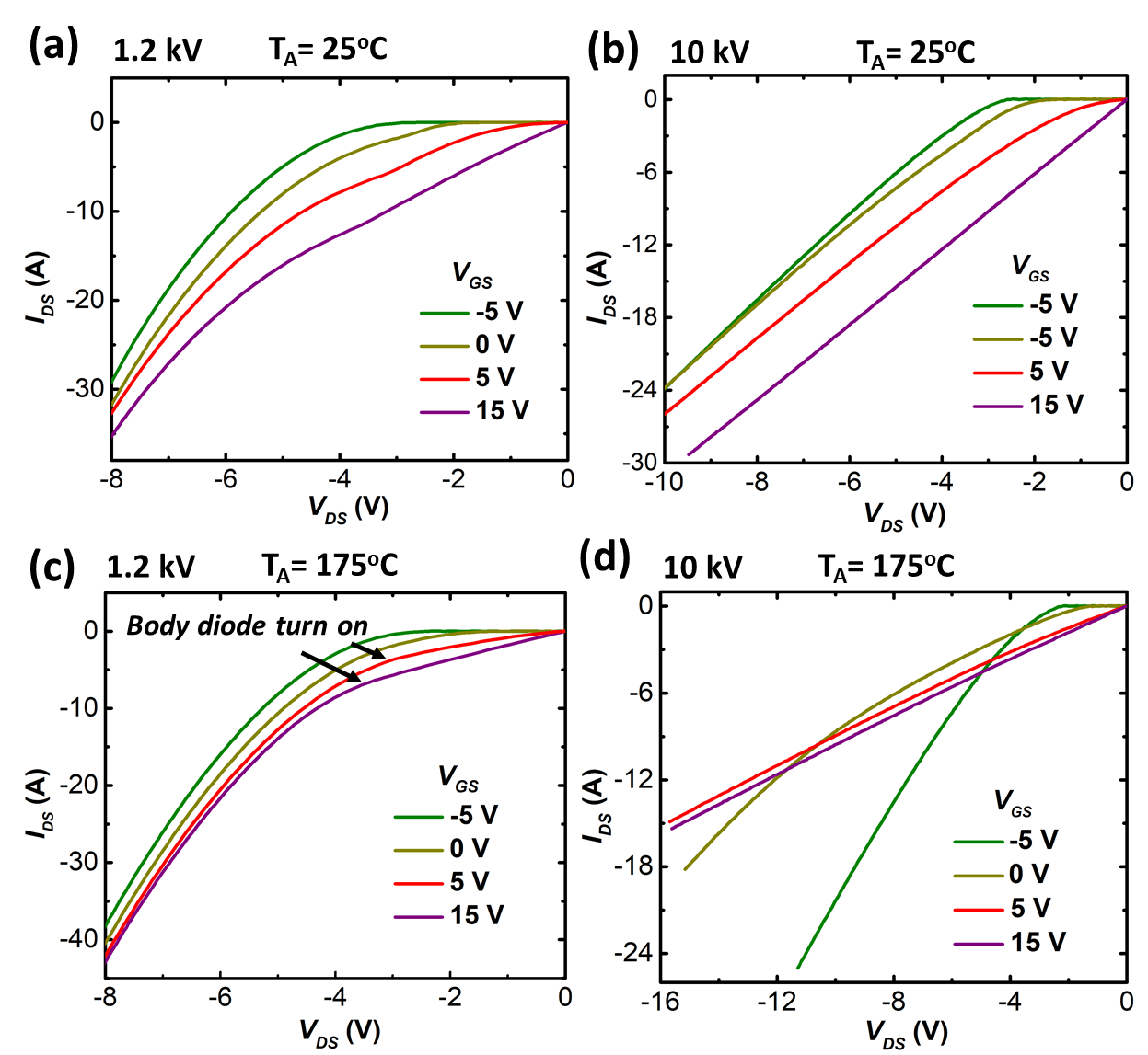
Fig. 1. I-V characterization of 1.2 kV and 10 kV SiC planar MOSFET under 25° C and 175° C.
Fig. 1 shows the 3rd-quad I-V characterization of an 1.2 and 10 kV SiC planar MOSFET at different VGS (-5 V15 V) under different temperatures (25° C, 175° C). For 1.2 kV at both temperatures, VGS > Vth gives a lower VF3rd since both the MOS channel and the body diode are conducting current. However, for 10 kV devices, at 175° C, crossovers among the I-V curves can be observed. This phenomenon can be explained by the clamping effect on the body diode: with the MOS channel path conducting current, due to the potential distribution inside device cell, a VBD-on higher than the body diode turn-on voltage is required to turn on the body diode. This VBD-on increases with device voltage rating and can be calculated as VBD-on=VF[1+ RDRIFT/(RMOS + RJFET)].
To find the optimal gate control bias in the 3rd-quad conduction, a dc-dc buck converter was built up using a 10 kV SiC MOSFET half-bridge power module. The circuit schematic and the test setup are shown in Fig. 2(a) and (b). From the test waveform shown in Fig. 2(c) and (d), at 50° C, VGS of 15 V provides lower VF3rd for the low-side MOSFETs. However, at 150° C, VGS of -5 V provides lower VF3rd. Note the same reverse recovery loss is expected for two VGS controls due to the need for dead time (VGS of -5 V). This indicates that a negative VGS leads to the minimal loss for 3rd-quad operation of 10 kV SiC MOSFETs at high temperatures.
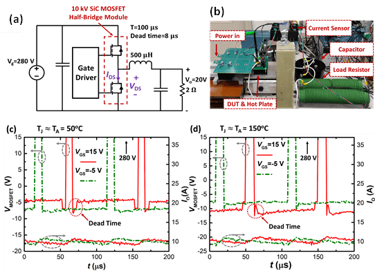
Fig. 2. (a) and (b), buck converter setup, (c) (d) test waveforms.
