LIBRARY
A High-Density Single-Turn Inductor for a 6 kV SiC-based Power Electronics Building Block

modules.
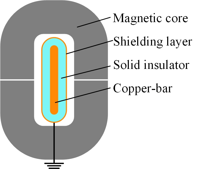
The inductor design begins with a comprehensive comparison of all the possible design solutions, including air-core and magnetic- core, single-turn and multiple-turn, air-insulation and shielded solid- insulation. The single-turn, magnetic-core structure with shielded solid-insulation (shown in Fig.1) is concluded to be the most suitable solution for lower power loss, smaller volume and more reliable in- sulation performance.
The design process is then followed by a multi-objective optimization of geometric dimensions and magnetics through a trade- off among power loss, volume, and parasitic capacitance. Under optimal solutions, the power loss, volume and parasitic capacitance from conductor to shield are calculated to be 14.17 W, 0.364 L and 127.22 pF.
As mentioned earlier, a shielding layer is employed to facilitate a compact and reliable insulation design; however, it has some side effects that need to be carefully handled. The first side effect is the extra loss on the shield caused by the leakage magnetic field near the air gaps. It is mitigated by a selection of shield conductivity and thickness based on the FEA simulation results. The second side effect is the high electric field stress on the shield fringes caused by the concentrated equipotential lines at the shield edges. It is solved by the proposed double-layer shield termination structure comprising of a high-permittivity stress control layer and a low-permittivity additional layer (Fig. 2(c)). The third side effect is the grounding current caused by the parasitic capacitance between the conductor and the shield, and the high dv/dt switching transient on the conductor. This issue is addressed by a well-designed grounding current damping resistor on the grounding path.
Finally, a prototype was fabricated in the lab using a copper bar with rounded edges, epoxy-bonded mica paper tape and conductive coating. The experimental performance is demonstrated as well. The partial discharge inception voltage (PDIV) of the inductor is measured to be 7.02 kV under a 60 Hz excitation. The measured input impedance matches the simulation up to 11 MHz. The converter level tests were done by connecting the inductor in series with the load inductor in the pump-back test setup, and the results show the trade-off between the effectiveness and compromise of the proposed grounding current reduction method.


