LIBRARY
A Compact High-Power Single-Turn Inductor for 6 kV SiC-based Power Electronics Building Blocks

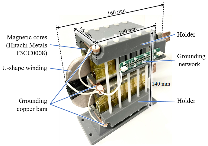
This work presents the design, construction, evaluation, and testing of a single-turn inductor for a 6 kV PEBB using 10 kV SiC MOSFET modules. Among all the design solution candidates, the single-turn magnetic core structure with shielded solid insulation is selected to be the most suitable solution for the given specifications. The U-shape winding was proposed to better coordinate with the overall PEBB structure. A grounded shielding layer is applied on the solid insulator surface to achieve high compactness, and issues arising from the shielding layer were comprehensively addressed. The grounding path of the shield was designed so that the displacement current has minimum impact to the PEBB (loss, EMI, etc.). Fig. 1 shows the overall inductor prototype.
When fabricating the inductor winding, two methods (resin rich and epoxy encapsulation) were used and compared. The resin rich method uses the resin bonded mica tape to wrap on the copper bar, which is followed by hot press and oven curing. The encapsulation method, as a contrast, requires a particularly designed and 3D-printed mold for fabrication. An epoxy encapsulant with proper properties was selected. It was found that the encapsulation method takes significantly less fabrication time while achieving the similar PDIV to the resin rich method.
The performance is experimentally demonstrated. The PDIV of the inductor is measured to be 5.16 kV under a 60 Hz excitation. The measured common-mode and differential-mode impedances match the simulation beyond 10 MHz. The converter level tests were done after the inductor was integrated to a 6 kV PEBB prototype. Fig. 2 shows the current and loss on the grounding network with varying dv/dt levels, demonstrating the effectiveness of the proposed grounding strategy.
This work also evaluates the application with higher current requirements.


