LIBRARY
Design of a High-Density Integrated Power Electronics Building Block (iPEBB) Based on 1.7 kV SiC MOSFETs on a Common Substrate

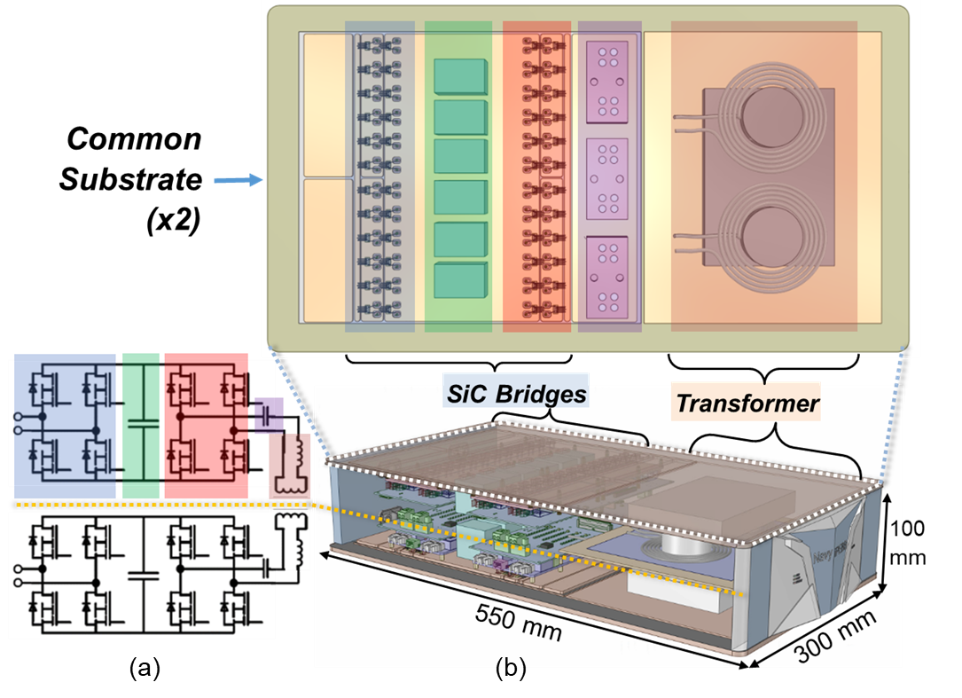
The primary and secondary side of the iPEBB have an identical common substrate, which simplifies manufacturing and reduces cost. This will allow the iPEBB to be mass produced and serve as the backbone of the power distribution system on future electric ships. The iPEBB is intended to be inserted into a rack, which will provide cooling to the top and bottom substrates, and hence the components mounted to them. Thermal, mechanical, and electromagnetic finite element analysis (FEA) simulations were performed to identify suitable substrate materials, dimensions, and layouts, while also minimizing the weight.
To verify the design, 1.7 kV SiC MOSFET half-bridges with Si3N4 and ODBC substrates have been packaged(Fig. 2(a) and 2(b)). The half-bridges will be tested in a quasi-square wave, zero-voltage switching (QSW-ZVS) buck testbed shown in Fig. 2(c). ZVS reduces the switching losses, enabling the 1.7 kV half-bridges to operate in the hundreds of kilohertz range. The testbed was designed to enable thermal imaging of the SiC MOSFET die during operation. These temperature measurements will be used to verify the thermal models. The proposed design and state- of-the-art substrate materials aid in the realization of the iPEBB, which will advance future electric transportation systems.
This work was supported by the Office of Naval Research (ONR) with the grant number N00014-16-1-2956.


