LIBRARY
High Power Density Design of Power Electronic Interrupter in Hybrid DC Circuit Breaker

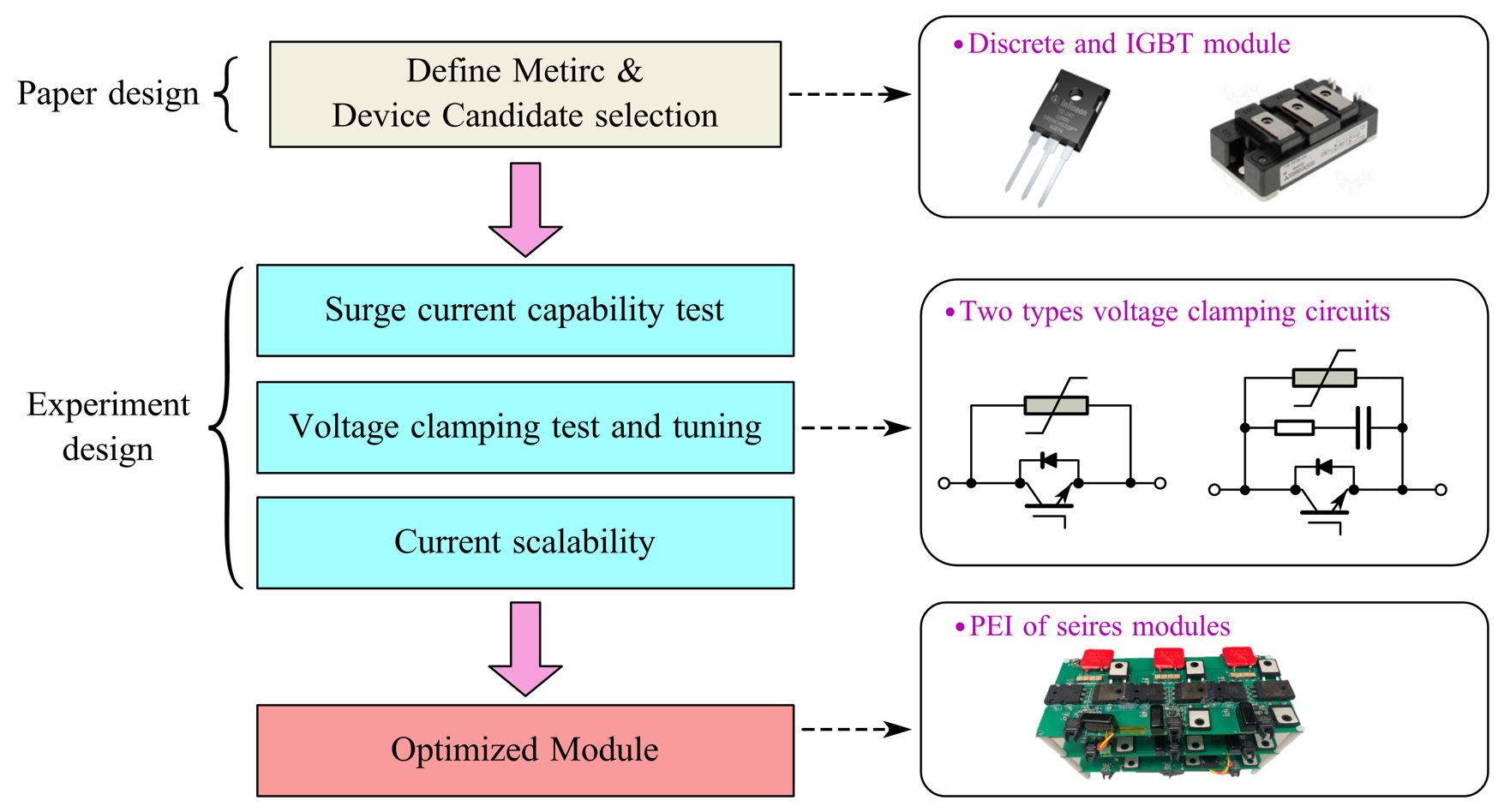
For the blocking voltage requirement, single IGBT is far from meeting the demand of 12kV, so series device is required. Traditional PEI usually adopts series device parallel with a concentrated voltage clamping circuit for energy absorption. Then additional voltage balancing circuits such as a passive snubber or an active gate driver, are designed to protect each device from exceeding withstand voltage. However, in dc circuit breaker, the function of the voltage clamping circuit overlaps with the voltage-balancing design. So the voltage clamping component can be divided into small components and paralleled with each device, which can be regarded as one module. In this way, the consistency requirements for devices are low and higher voltage could be achieved by the series of more modules. Besides, if one module is damaged during operation, the other module will not be exposed to higher voltage so that the cascading damage could be avoided. The modular design procedure was shown in Fig. 2.
According to this procedure, a small sized module with two parallel 1.7 kV discrete IGBTs are selected as main switches. The RC snubber and MOVs are carefully designed to guarantee no tail current bump and sufficient turn-off voltage margin. Different methods are also utilized to suppress the current bumps to avoid device failure. In the module integration stage, the power supply structure and staged turn-off strategy are investigated to improve the power density and breaking time. Experimental results at 12 kV and 1 kA are provided to verify the operation of the prototype.


