


LIBRARY
Double-Side Cooled Medium-Voltage Power Module with Sintered-Silver Joints Demonstrated in an 8-kV Silicon Carbide Diode Module
Year: 2021 | Author: Zichen Zhang | Paper: S5.2
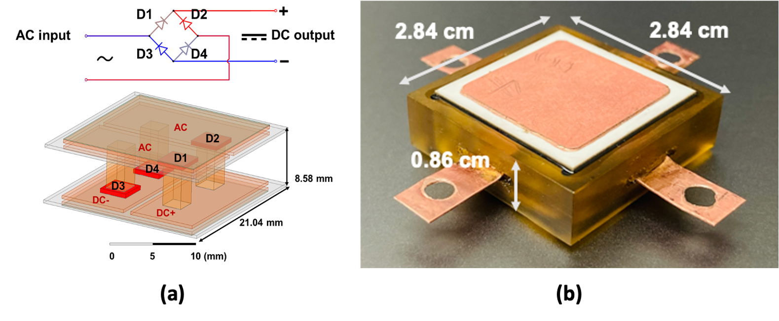
Fig. 1. SEQ Fig.1 (a) Schematic of the double-side cooled 8-kV SiC diode full-wave module and its equivalent circuit. (b) Prototype of the 8-kV SiC diode full-wave rectifier module.
In this work, we implemented the two packaging innovations for the design and fabrication of an 8-kV SiC full-bridge diode rectifier module. Fig. 1(a) is a schematic of the module layout. The device chips were sandwiched between two patterned direct-bond-copper (DBC) substrates. Die-attach and metal-post bonding were done by silver sintering. Steady-state thermal simulations were run to verify the benefit of double-side cooling. Electrical and electric field simulations and analyses were performed to minimize the loop inductances and guide the insulation design. The packaging concept was implemented in assembling an 8-kV SiC diode full-wave rectifier shown in Fig. 1(b). The electrical testing results of the module shown in Fig. 2, validated the package design and fabrication.
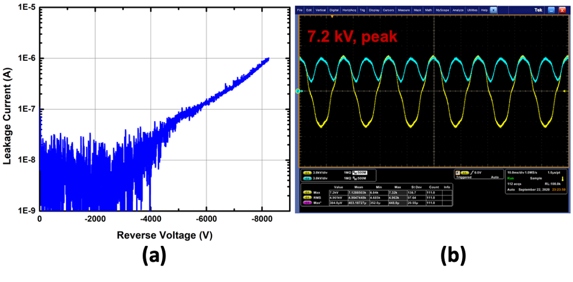
Fig. 2. (a) Reverse I-V characteristics of Diode 4 (labeled in Fig. 1(a) as D4) after packaging. (b) Output dc waveform (blue) under 60 Hz sinusoidal ac input (yellow) with a 7.2 kV peak value.
