LIBRARY
Integrated Power Electronics Building Block Circuit Design and Analysis

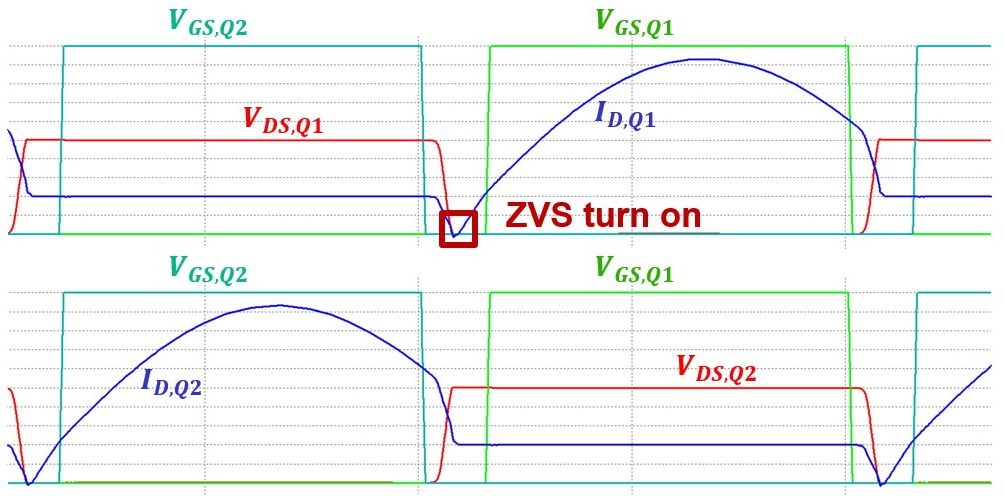
A 500 kHz, 250 kW dc-dc CLLC resonant converter was simulated in this work. The magnetizing inductance, and the primary and secondary side leakage inductances of a 500 kHz transformer were extracted using FEA simulations. Nine 1.7 kV SiC MOSFETs are used in parallel to achieve 98.5% efficiency. The simulated conduction, switching, and transformer losses were found to be 2.13 kW, 0.75 kW, and 1.15 kW, respectively. The deadtime was calculated such that the output capacitance of the MOSFETs have sufficient time to discharge/charge to reduce switching loss. Fig. 2 shows the simulated waveforms of the CLLC converter operating in ZVS.
A high-frequency ZVS-buck converter was also designed and simulated. This converter will be used to test the high-frequency capability of a custom 1.7 kV SiC MOSFET module and verify the ZVS operation and simulated losses. These test results will be used to inform the CLLC converter loss and ZVS operation.
This work was supported by the Office of Naval Research (ONR) with the grant number N00014-16-1- 2956.


