LIBRARY
Design and Analysis of a PCB Embedded SiC Half-bridge Module

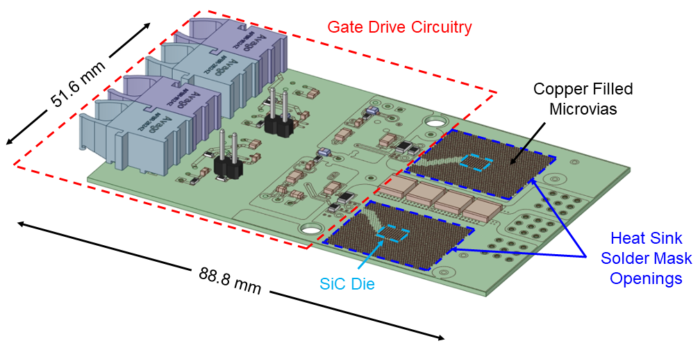
The design of this module (Fig. 1) is based on maximizing the benefits and understanding the trade-offs of the die PCB-embedding technique. The two die are kept far enough apart to minimize thermal coupling, while also maintaining a small power loop. The gate drive circuitry is included in the module to ensure a small gate loop. Copper-filled microvias are used to thermally connect the inner and outer copper layers between the die and the solder mask openings. Copper planes that are electrically connected to the die are designed to maximize power density, while allowing for sufficient heat spreading.
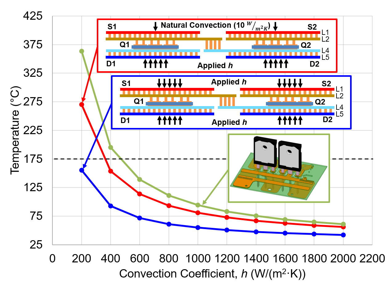
Thermal and electrical FEA simulations were performed on the module. The power and gate loop inductances are 1.8 nH and 2.0 nH, respectively. The double-sided thermal resistance of the embedded half-bridge module is 0.27° C/W. As seen in Fig. 2, the PCB-embedded module has a lower junction temperature than a conventional TO-247 wire-bonded package under similar conditions.
The PCB-embedded, half-bridge module presented here is expected to outperform industry-standard packages both thermally and electrically. Future experimental work includes thermal impedance measurement and analysis, power cycling tests, failure analysis, and converter testing to further explore the benefits and trade-offs of the PCB-embedded 1.2 kV SiC power module.


