LIBRARY
Design of a 24 kV PCB Based DC Bus
Year: 2022 | Author: David Nam | Paper: H-S5.2
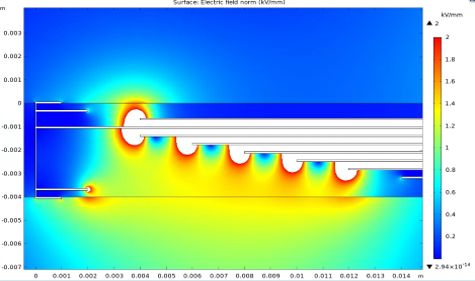
Fig. 1. Cross-sectional view of a PCB with a high voltage layer stack up
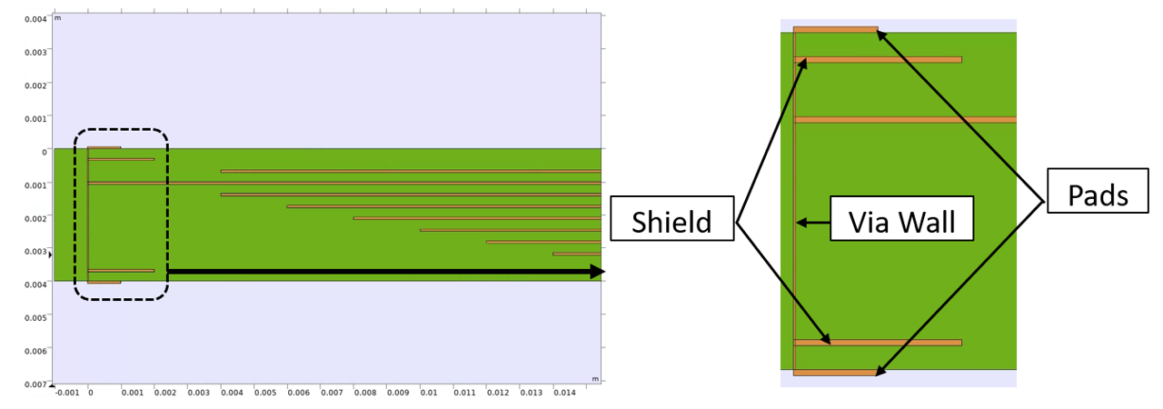
Fig. 2. Verification of high voltage PCB design through FEA simulations

The Center for Power Electronics Systems (CPES), with annual research expenditures of $6-7 million dollars, is dedicated to improving electrical power processing and distribution that impact systems of all sizes – from battery-operated electronics to vehicles to regional and national electrical distribution systems.
Discover More About CPESThis spring, CPES welcomes Dr. Ming Xu back to the center as professor a...
CPES is proud to congratulate Tianyu Zhao on the successful defense of h...
The Center for Power Electronics Systems (CPES) is proud to congratulate...
CPES Industry Webinars offer engineers from member companies the opportu...

CPES continuously releases news regarding our conferences, faculty, and students. We also provide a list of events for webinars, conferences, and many other facets!

The CPES Industry Consortium cultivates connectivity among researchers in academia and industry, and creates synergy within the network of industry members. Our industry consortium is the backbone of our strong technology transfer success.
Check Out the CPES Industry Consortium
Our library includes the Center's technical papers published in conference and journal papers, presentations, recordings, thesis and dissertations produced by graduates, and a research volume series compiled by CPES faculty.
See What Publications CPES Has On Offer
One of the Center's missions is to develop and education program that promotes multi-disciplinary, team-driven, and systems-oriented training to CPES students, as well as provide continuing education opportunities to our industrial partners.
Learn About Our Education Opportunities