


LIBRARY
Design and Control of High Power Wide Gain Range LLC Converters
Year: 2022 | Author: Chunyang Zhao | Paper: H-S4.4
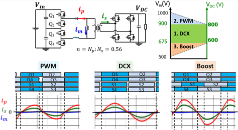
Fig. 1. Circuit topology and waveforms of three-mode operations
However, in high-power wide-gain-range applications, there is hardly a solution to meet both constrains. Thus, multi control methods are combined to solve the problem. In general, the con-verter will operate in DCX mode when the input voltage is in the nominal voltage range to maxim-ize the peak efficiency and operate in Boost mode when the input voltage is lower than nominal values to boost gain and operate in PWM mode when the input voltage is higher than nominal values to reduce switching frequency and device losses.
Fig. 1. shows the topology and key waveforms of three-mode operations. 3D gain curves and operating path are shown in Fig. 2.

Fig. 2. 3D gain curves and operating path
