LIBRARY
Overvoltage Ruggedness and Dynamic Breakdown Voltage of P-Gate GaN HEMTs in High-Frequency Switching up to Megahertz

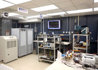
Fig. 1 (a) & (b) show the test circuit and a photo of the test setup. Fig. 1 (c) & (d) illustrates the working principle of the ACC via the LTspice simulation at a 400 V input voltage (Vin), 1 MHz FSW and 0.5 duty cycle. when the ACC intervenes. The ACC works at the same FSW as the converter. In each switching cycle, ACC turns ON at the end of the first VDS overshoot, transferring the surge energy to the ACC loop and regulating the overvoltage waveform to contain only one high VDS overshoot pulse. It turns OFF before the top switch turns ON. The energy stored in Lair is fully dissipated via the clamping circuit in each cycle, and a stable peak VDS can be achieved.
Fig. 2 summarizes the testing results. While the HD-GIT shows a nearly FSW-independent dynamic BV, the SP-HEMT shows a decreasing dynamic BV at higher FSW, e.g., 270-V lower when FSW increases from 2 kHz to 1 MHz. The change of BV with FSW can be explained by the time-dependent electron trapping and the impacted dynamic BV of GaN HEMTs. In HD-GIT, an additional p-GaN is electrically connected to the drain metal, holes are injected from the drain under high VDS, which neutralize the acceptor traps in the GaN buffer and alleviate the peak E-field at the drain side. On the contrary, in SP-HEMT the filling of acceptor traps in the GaN buffer results in a dynamic BV lower in higher FSW test.


