


LIBRARY
Thermal and Thermomechanical Analysis of a 10 kV SiC MOSFET Package with Double-Sided Cooling
Year: 2022 | Author: Mark Cairnie | Paper: H-S1.1
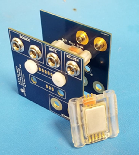
Fig. 1. 10 kV/25A discrete SiC MOSFET package measuring 32 x 31 x 7 mm3 shown mounted to two PCB busbars
Parallel heat flow paths are provided through the top and bottom of the die by means of wirebond-less molybdenum interconnects that serve as both the electrical connection to the die (replacing conventional wirebonds) and conduct heat from the die to an upper substrate. High thermal conductivity materials such as aluminum-nitride ceramic and sintered silver die- and post-attach are used to reduce the junction-to-case (θjc) thermal impedance. Special care is taken to manage thermomechanical stress inside the package as materials with high-thermal conductivity generally tend toward larger Poissons ratio and thus can exhibit larger thermomechanical stress-es due mismatches in the coefficient of thermal expansion. This leads to a trade-off between low thermomechanical stress and low θjc. In the work, finite element simulation via ANSYS® and Abaqus® (Fig. 2) are used to evaluate this trade off and select appropriate materials to ensure high thermal performance without sacrificing reliability.
The θjc of the assembled package was characterized on a JEDEC 51-14 compliant test bed and experimentally determined to be 0.17° C/W overall, 0.25° C/W and 0.57° C/W on the lower and upper cooling surfaces respectively. The package was run continuously with a dc channel current of 150 W to pin the junction temperature at a constant 150° C for 30 minutes, after which no degradation of the silver sinter bond lines was observed. This work demonstrates the viability of double-sided cooling for packages up to 10 kV and the performance improvements that can be gained over the existing state-of-the-art.
