LIBRARY
Reduce-Order Analysis and Circuit-Level Cost Function for the Numerical Optimization of Power Electronics Modules

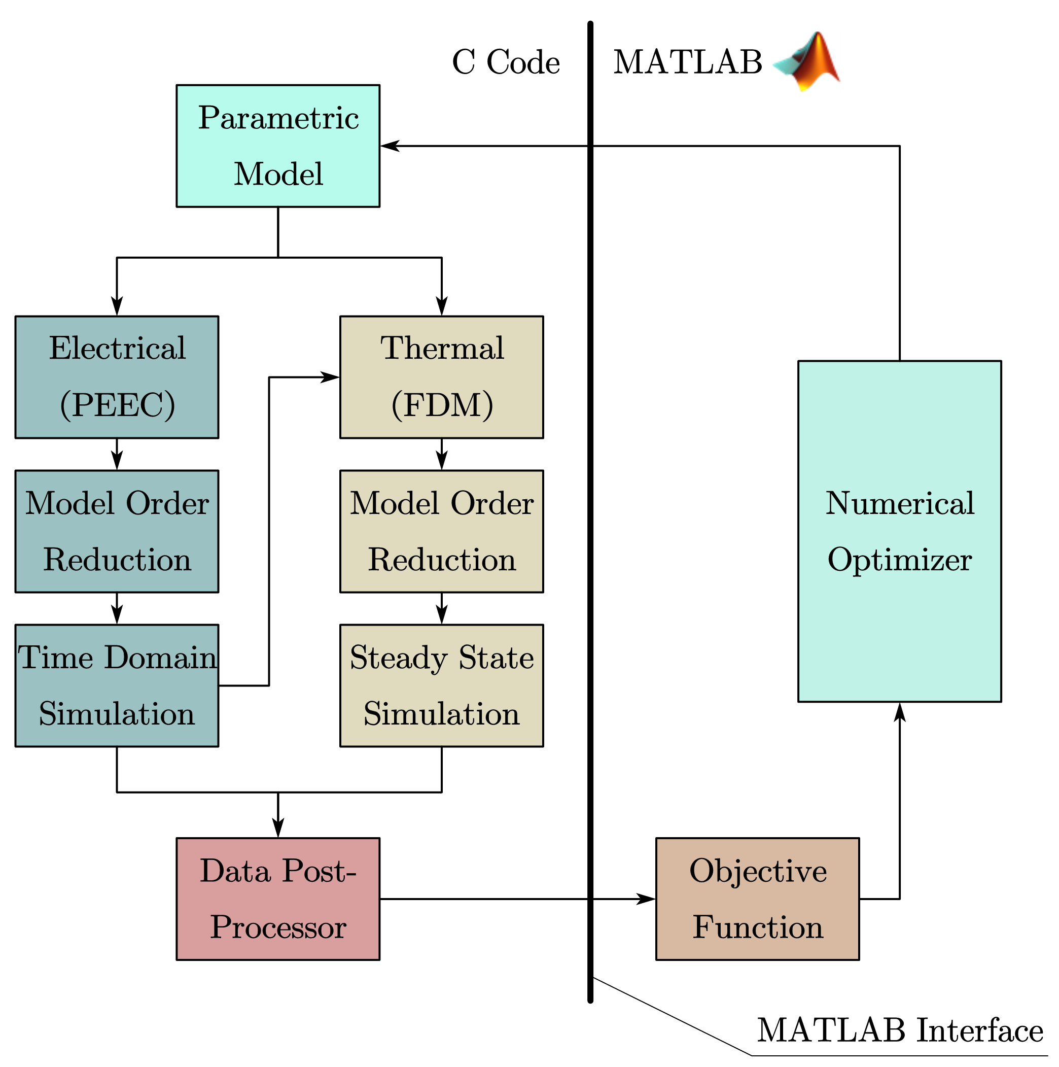
Employing reduced-order PEEC as the forward solver, as opposed to more conventional fi-nite element techniques, provides both decreased simulation time (up to 100x) as well as access to time domain simulation outputs of the package operating in a converter. This enables the de-signer to efficiently model the voltage and current transient stresses on the package during con-tinuous operation of the device and relate these stresses to the material and geometric design decisions. The addition of time-domain simulation results in the optimization allows for a wide range of possible cost functions that prioritize performance of the package in a converter.
One such cost function is proposed in the work and demonstrated on a 10 kV/25 A discrete SiC MOSFET package with double-sided cooling (Fig. 2). The proposed cost function utilizes the time domain outputs of the reduced-order PEEC to optimize the position of the die in the pack-age based on the power noise spectrum emitted by the package during 100 kHz hard-switching. On standard desktop hardware, the optimal die position was determined in ~30 iterations of the optimizer at a rate of 15 min/iteration. During each iteration, a time-domain simulation electrical simulation (10 μs duration and 100,000 time steps) and a steady-state thermal simulation were completed. This work demonstrates both the reduction in computational time and the improved flexibility of power electronics package optimization enabled by reduced-order PEEC.


