LIBRARY
Active Gate Drivers for EMI and dv/dt Control

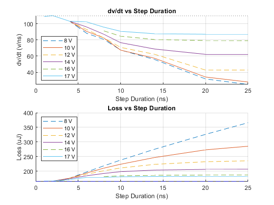
When looking at reduction in dv/dt, simulations were performed using the C2M0080120D CREE SiC MOSFET. From these simulations the intermediate step voltage and duration of this voltage were adjusted. The results are plotted in Fig. 2 which shows the dv/dt being reduced from ∼ 110 V/ns to ∼ 30 V/ns (with an 8 V applied step). This represents a reduction of almost 73%. These results show a noticeable range in dv/dt reduction with an active driver. Through the introduction of additional intermediate voltage steps the results did not show any noticeable improvement in this area.
From the perspective of loss Fig. 2 shows a clear trend as the step duration increases the losses also increase until a point where the dv/dt no longer is reduced, then loss remains constant.
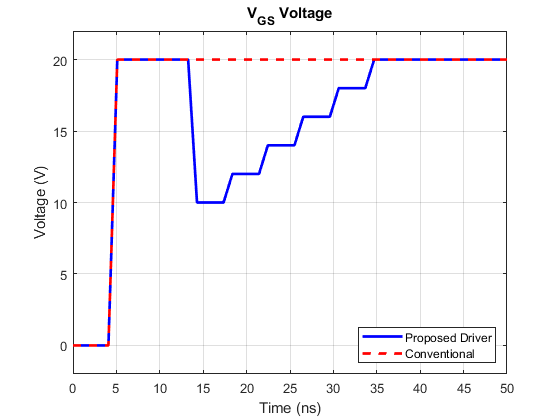
A final improvement noted in initial simulations is with the peak gate current during the drain voltage fall region. With the introduction of additional voltage steps in the gate driver voltage that achieved the same dv/dt, the peak gate current in this region was reduced and the current stayed at a more constant value.


