LIBRARY
A PCB-Embedded 1.2 kV SiC Half-Bridge Module for EV On-Board Charger Applications

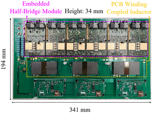
Following the design and manufacturing, the PCB-embedded half-bridge modules were experimentally tested to measure their performance. The source-side and drain-side junction-to-case thermal resistances were measured to be 0.41 K/W and 0.17 K/W, respectively, using the JEDEC 51-14 standard and a Phase 12 B Thermal Analyzer. Under similar operating conditions, the PCB-embedded half-bridge module achieved 5.6 times lower voltage overshoot during turn-off and 0.5% higher efficiency than a TO-247 package containing the same SiC MOSFET. With the help of soft switching and low loop inductances, the measured peak efficiency and power density of the 22-kW three-phase ac-dc converter prototype with six PCB-embedded half-bridge modules seen in Fig. 2 are 98.2 % and 182 W/in3, respectively.
The experimental results obtained in this work provide evidence that PCB-embedding is a viable packaging method for use in electric vehicle OBCs. The integrability, power density, and thermal and electrical performance afforded by PCB-embedding makes it a great candidate as a packaging method for SiC MOSFETs. The large-scale adoption of PCB-embedding in power converters hinges on reducing manufacturing costs and gaining a better understanding of the failure mechanisms seen in power and thermal cycling.


