LIBRARY
PCB Technology Comparison Enabling a 900V SiC. MOSFET Half Bridge Design For Automotive Traction Inverters

The three PCB technologies compared are a heavy copper PCB with copper inlays for better thermal conductivity from junction to heatsink, a ceramic inlay PCB, and an em-bedded SiC. die PCB. The PCB technologies are compared based on the thermal conductivity path from junction to heatsink, the high current capability, and the switching transient overshoot voltage influenced by current commutation loop stray inductance.
Finite element analysis is carried out in Ansys Icepack to analyze the thermal resistance path from junction to heatsink. The junction temperature must not exceed 150 °C. The results indicate that the junction temperature exceeds the threshold for the copper inlay PCB. The ceramic inlay and embedded die PCB have a low thermal resistance allowing the junction temperature to stay below 150 °C.
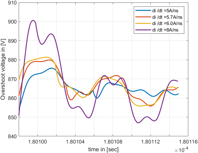
The current density should not exceed 5 A/mm2 to allow for passive cooling of the DC link capacitor. Finite element analysis shows a current density of 43.3 A/mm2 due to thin copper layers. The embedded die PCB has a current density of 4.3 A/mm2. Thus, switching transient overshoot voltage is further analyzed. The PCB parasitics are derived from Ansys Q3D simulations and imported into SPICE simulations. The resulting switching transient is depicted in Fig. 1. The overshoot voltage is 33 V at a current slope of 5.7 kA/μs. Thus, the maximum drain-source voltage does not exceed the break down voltage of the 900 V SiC MOSFET.
The comparison shows that an embedded die PCB is suited for using 900 V SiC MOSFET for 800 V automotive traction inverter application. Further work includes testing the thermal conductivity and switching transients on a prototype.


