LIBRARY
Analysis of EMI Mitigation for SiC Power Modules Using an Integrated Common-Mode Screen

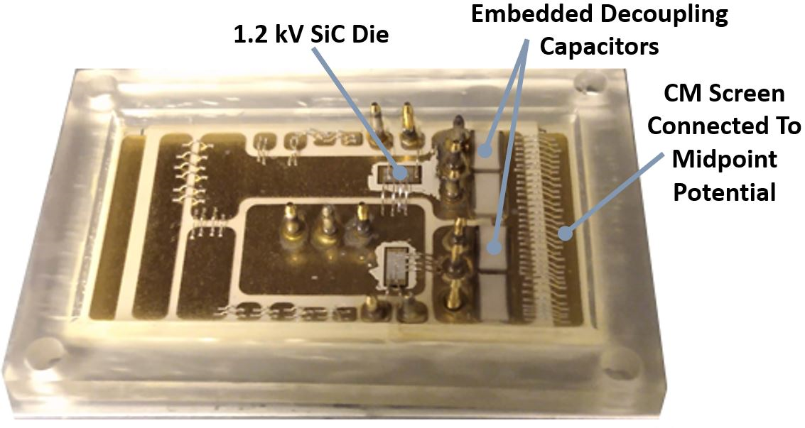
The hardware implementation of the embedded CM screen module architecture explored is shown in Fig. 1. The CM screen is formed by using a two-layer substrate and con-necting the middle layer to the power terminals. The current generated by the high dv/dt at the switching node of the half bridge is then redirected, reducing the current flowing through the baseplate. The amount of current diverted will depend primarily on the impedance of the CM screen path to the connected terminal. In this study, the embedded CM screen is shorted to the midpoint of the bus voltage, which is formed by the series connection of embedded capacitors. The midpoint connection to the CM screen further helps by evenly distributing the electric field in the ceramic layers.
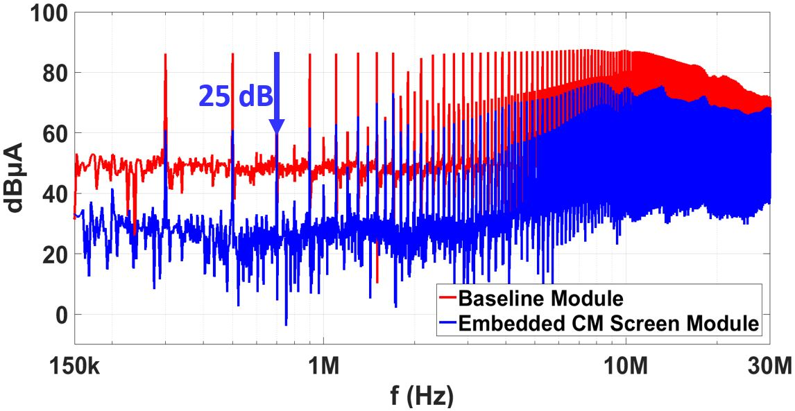
To evaluate the EMI noise generated, a baseline module with no embedded CM screen and decoupling capacitors and the module shown in Fig. 1. are switched in a buck converter topology with a switching frequency of 100 kHz, input / output voltage of 600 V / 300 V, and an output current of 12 A. The EMI noise current flowing through the baseplate of the modules is measured and compared as shown in Fig. 2. Initial test results show that due to the introduction of the embedded CM screen and decoupling capacitors, noise mitigation of up to 25 dB is observed in the conducted EMI frequency range.


