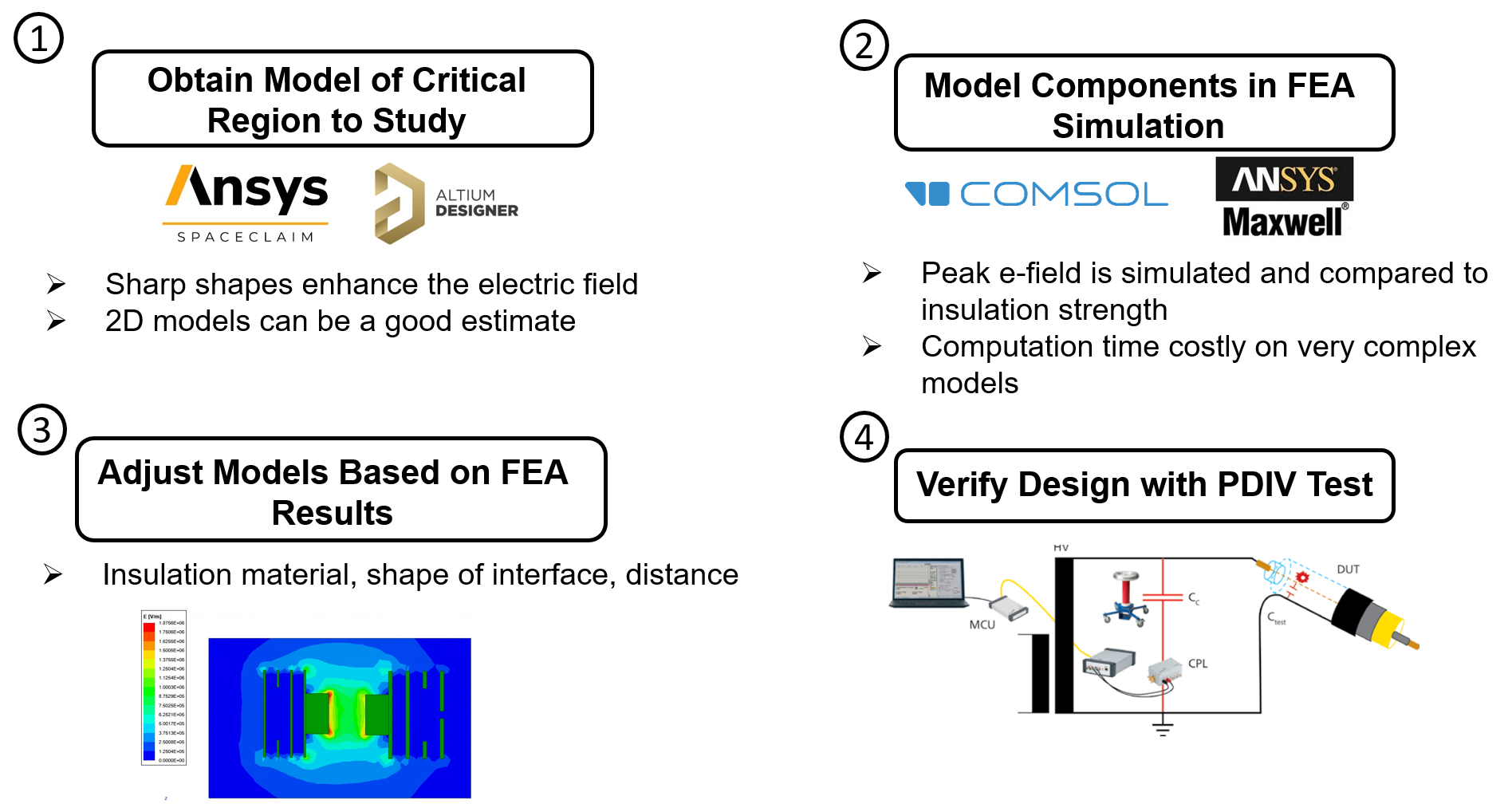
Fig. 1. Design principles for an electric field constrained converter
The recent development of 10 kV silicon-carbide (SiC) MOSFETs has enabled the high-power-density design of medium-voltage converters. As a result of increased voltage levels and higher densities, the presence of high electric field intensities throughout the converter require deliberate considerations in terms of insulation design and layout coordination. This paper focuses on the techniques and verification of finite element analysis (FEA) -based insulation design of a 22 kV, three-phase five-level flying capacitor converter, which serves as a base for the seven-level converter. The procedure for designing the converter, with consideration given to the peak electric field, is shown in Fig 1. This paper also proposes a new implementation of a 22 kV printed circuit board (PCB)-based busbar. Through careful planning of the component layout selection by FEA analysis and experimental validation, the overall structure of the PCB-based dc bus was determined. The PCB design consolidated previous techniques that had been constrained by the electric field of PCB-based dc buses, and provides a new structure that addresses the unique challenges of a flying capacitor converter. In addition, modifications to the five-level flying capacitor converter are made to enable a seven-level configuration, the test setup for which is shown in Fig 2. The motivations and methods for setting up the seven-level converter are discussed. Necessary design considerations to achieve this level of operation are discussed in detail. Finally, plans to develop a permanent seven-level converter setup are discussed.
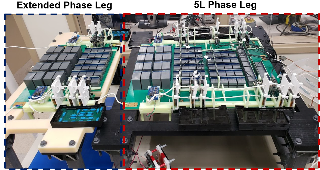
Fig.2. Seven-level converter experimental setup.


