


LIBRARY
Partial Phase Overlap Control for 48V/1.8V Single Stage Series Capacitor Buck Converter
Year: 2023 | Author: Adhistira Naradhipa | Paper: H5.5
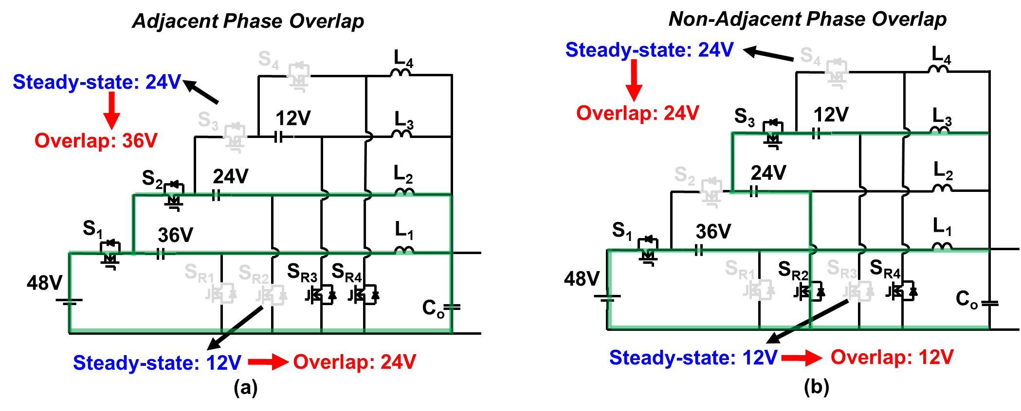
Fig.1. 48V SCB converter (a) adjacent phase overlap, and (b) non-adjacent overlap.
The proposed control scheme is based on constant-on-time (COT) control with a phase manager. Partial phase-overlap control will take over at the high load-step-up where the control command becomes saturated, and the minimum off-time will determine the duty cycle. The phase overlap can be achieved by setting the minimum off-time value to be smaller than the on-time. To avoid overlap of adjacent phases, a simple logic circuitry is added to the minimum off-time generator. Therefore, only non-adjacent phase overlap is allowed, and device voltage stress increase is avoided. Fig. 2 (a), (b), and (c) show experimental waveforms at the load-step-up transient with no overlap, adjacent overlap, and with non-adjacent overlap, respectively. Both phase-overlap methods have similar transient performance, which is better than the no-overlap method. However, the adjacent overlap increases device voltage stress, whereas the device voltage stress is kept the same as in the steady state using the proposed partial phase-overlap method.
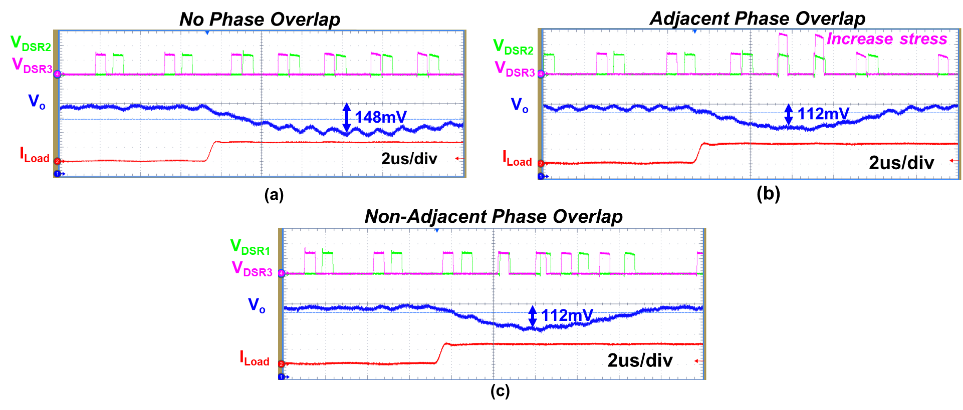
Fig.2. Load-step-up transient experimental waveforms: (a) no phase overlap, (b) adjacent phase overlap, and (c) proposed non-adjacent phase overlap.
