LIBRARY
Electro-Thermal Optimization of Common-Mode Screen for Organic Substrate-Based SiC Power Module
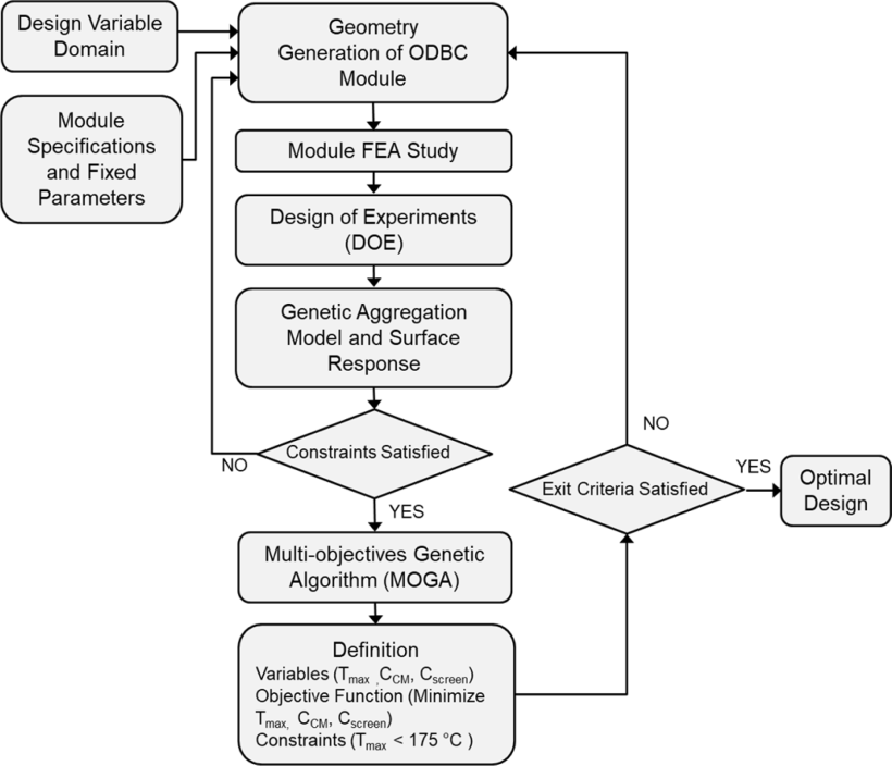
ANSYS Workbench's analysis tool was used to perform the optimization on the organic direct bonded copper (ODBC) module and balance the electromagnetic interference (EMI) and thermal tradeoffs. The optimization model considered the copper (Cu) thickness, the pad width, and the dielectric thickness of the different module layers. The model's goal was to minimize three key factors: 1) maximum temperature, 2) capacitance from switching node to screen (CCM), and 3) the capacitance from the screen to the baseplate (Cscreen). The power module optimization flowchart is shown in Fig. 1. The ANSYS multi-objective genetic algorithm tool was used for the analysis. The model generated 7000 samples initially and went through 20 iterations with 1400 samples per iteration. In the end, three candidate points were selected from the Pareto-front.
The optimization model increased the top pad thickness to 5.5 mm, enabling better heat spreading. In addition, the ODBC's dielectric 1 and 2 were optimized to be 75 ?m and 93 ?m, respectively, to balance thermal performance with the capacitive coupling of the module. The resultant outputs from this design are a maximum temperature of 174.02°C, a CCM of 0.309 nF, and a Cscreen of 1.173 nF.
Simulation results show that the CM screen is effective for organic substrates. The multi-layer design, which the ODBC enables, allows for a high level of CM current containment. Optimizing the module let there be less capacitive coupling and enabled a ~25 dB noise reduction. Future work on fabricating the module and hardware verification will be completed.


