LIBRARY
Design And Fabrication Of An Inverter Module Co-Designed With Interfacing Busbar and Gate Driver

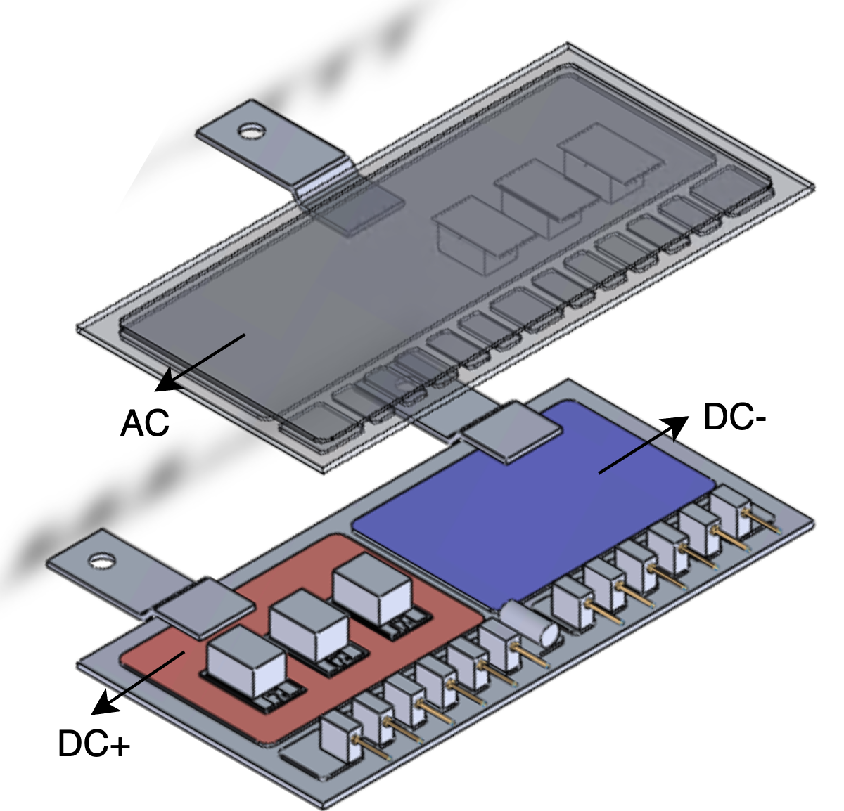
The design of the inverter module incorporates a double-sided cooling structure with three die per switch position. The module is designed with parasitic, thermal, and thermo-mechanical considerations to optimize the layout of the substrates and interfacing with the gate driver and busbar printed circuit boards (PCBs). Molybdenum posts are used as source interconnects to reduce parasitics inside the module and allow for better transient performance and a less complicated implementation of the double-sided structure. Wire bonding is used for the interconnected gate and kelvin to simplify the substrates' copper layout. Parasitic simulations are conducted on an ANSYS Q3D, allowing the post height to be increased to account for wire bonding and an embedded thermistor. The embedded thermistor enables health and degradation monitoring by measuring the internal temperature of the module.
The incorporation of six die in the module (three per switch position) in this structure makes the module longer, which raises concerns of bowing and deformations that may cause the source posts to disconnect from the phase-leg connection and incapacitate the module's performance. Simulations that can detail and compare the relative normal deformation arising from various substrate materials and copper thicknesses are pertinent. A mesh convergence study was performed, and 0.6mm aluminum nitride (AlN) was chosen as the substrate with 0.3mm copper plating on both sides, with 3mm source posts and 5mil-thick wirebonds. This module is intended to operate with >1 kV blocking voltage, <20 m&Omega RDSon, <0.2 K/W Rthj-c, and <20 ns switching to finally demonstrate a 1kV phase-leg Inverter operation. Commercially, this module is designed for applications comparable with those of the GE 1700V half-bridge module.


