LIBRARY
Design and Fabrication of Gallium Oxide Junction Barrier Schottky Diode

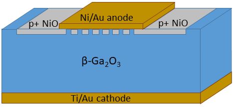
The semiconductor gallium oxide (Ga2O3), an ultra-wide-bandgap (UWBG) semiconductor (4.8 eV), has been researched heavily for vertical power diodes due to its favorable material properties including melt and homoepitaxial growth, doping control, and the prospect of a high breakdown field strength (6-8 MV/cm). However, due to the flat valence band and strong self-trapping of holes, the realization of p-type conductivity within Ga2O3 has thus far been unsuccessful. This means that a p-type semiconductor with favorable band offsets to Ga2O3 must be used in order to form a PN junction and JBS diode. Nickel oxide (NiO) has been shown to form a heterojunction with Ga2O3 due to its wide bandgap (3.7 eV) and p-type conductivity. NiO is most commonly deposited using reactive sputtering, where variation of the oxygen partial pressure allows for control of the hole concentration.
This work demonstrates the fabrication of a Ga2O3 NiO JBS diode, taking advantage of lower on-state power losses than a PN diode and a higher breakdown voltage than a Schottky barrier diode. It is the addition of the p+ regions that allows the JBS diode to achieve higher breakdown voltages than the Ga2O3 Schottky diode, the performance of which is limited by the Schottky barrier leakage current. A self-aligned fabrication process has also been developed, allowing for trench etching of the Ga2O3 followed by NiO deposition into the etch regions, with features as small as 1 μ m. A >1000 V Ga2O3 JBS has been achieved with state-of-the-art performance in Ga2O3 power rectifiers.
IMAGE1]


