LIBRARY
A 1.2 kV Embedded Die Half-Bridge PCB Design and Evaluation for Traction Inverter Applications
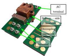
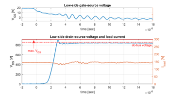
Fig. 1 depicts the embedded die PCB prototype. The embedded die technology enables the placement of bare SiC dies into the PCB. The usage of a PCB allows for a vertical integrated current-commutation loop rather than a lateral loop design of a standard power module. The die is sintered onto an 11x11mm2 copper lead frame. The lead frame is then embedded into the PCB and electrically connected with buried vias. The bottom-side and top-side prepreg materials electrically isolates the embedded inlay to the heatsink. Thus, a highly thermally conductive and electrically non-insulating interface material can be used. Double-pulse tests were conducted at a dc-bus voltage of 850 V and a drain current of 145 A to evaluate the embedded die PCB switching performance. Measurement results shown in Fig. 2 have a maximum overshoot voltage of 49.6 V during the turn-off switching transient at a switching speed of 69 V/ns. Additionally, thermal impedance tests, based on the JEDEC standard JESD51-14, were conducted. Both, high-side and bottom-side half-bridge MOSFET dies have a junction-to-case thermal resistance of 0.418 K/W and 0.625K/W , for bottom-side and top-side cooling respectively. The measured junction-to-case thermal resistance for double-sided-cooling equals 0.28 K/W per die.
