


LIBRARY
First demonstration of vertical superjunction in GaN
Year: 2023 | Author: Yunwei Ma | Paper: T2.1
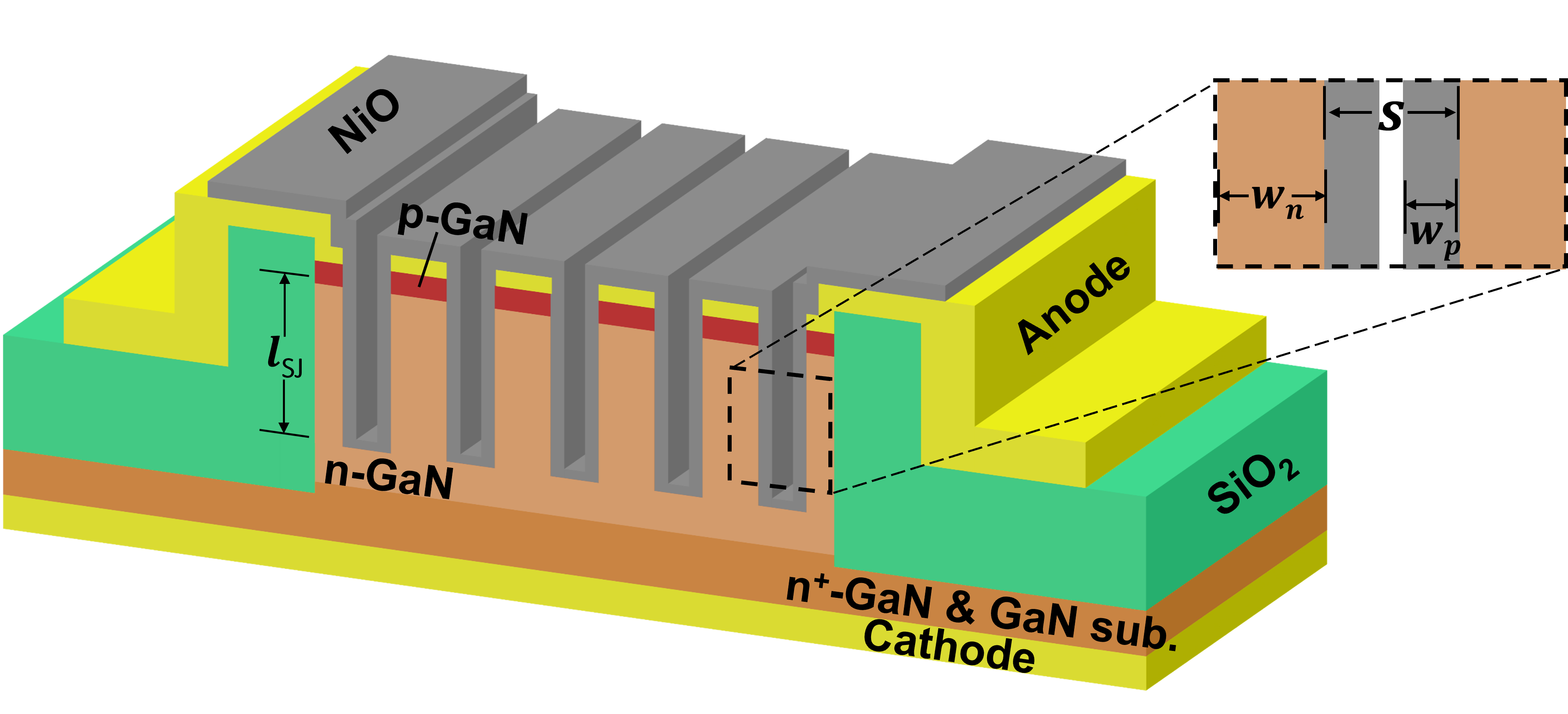
Fig.1 Cross-section view of GaN superjunction device
In this work, we demonstrated the first GaN vertical superjunction device by employing new p-type material: p-type NiO, and novel fabrication. Fig.1 shows the device cross-section view. More than 6 µm height with 1 µm width fin is fabricated by GaN dry etching to maximize breakdown voltage while minimizing specific on-resistance. A novel heterojunction PN pillar is fabricated by sputtering NiO on top of n-GaN fins. In ideal case, the amount of acceptor in NiO needs to balance the donor inside n-GaN fin in reverse condition. This is achieved by adjusting acceptor concentration in NiO by O2 percentage during NiO sputtering, as well as the n-GaN fin width during GaN etching. Such charge-balanced heterojunction PN pillars are used to manage the electric field without the need to use the conventional p-GaN regrowth process, which is still not matured. High blocking electric field (>2.6 MV/cm in GaN) has been demonstrated in the heterojunction, which allows for realizing high breakdown voltage.
As shown in Fig.2, our device shows breakdown voltage up to 1100 V, which is ~900 V higher than 1-D counterparts (190 V). Both GaN-on-GaN and GaN-on-Sapphire wafer show similar BV, the later one could promise a much lower fabrication cost. The devices total specific on-resistance is 0.3 mΩ*cm2. The drift region (which holds reverse voltage) specific on-resistance is 0.15 mΩ*cm2. The trade-off between the breakdown voltage and the drift region specific on-resistance breaks the theoretical limit of the 1-D unipolar GaN devices, and is expected to provide even better performance at higher voltage range. This work proves the great potential of GaN superjunction devices.
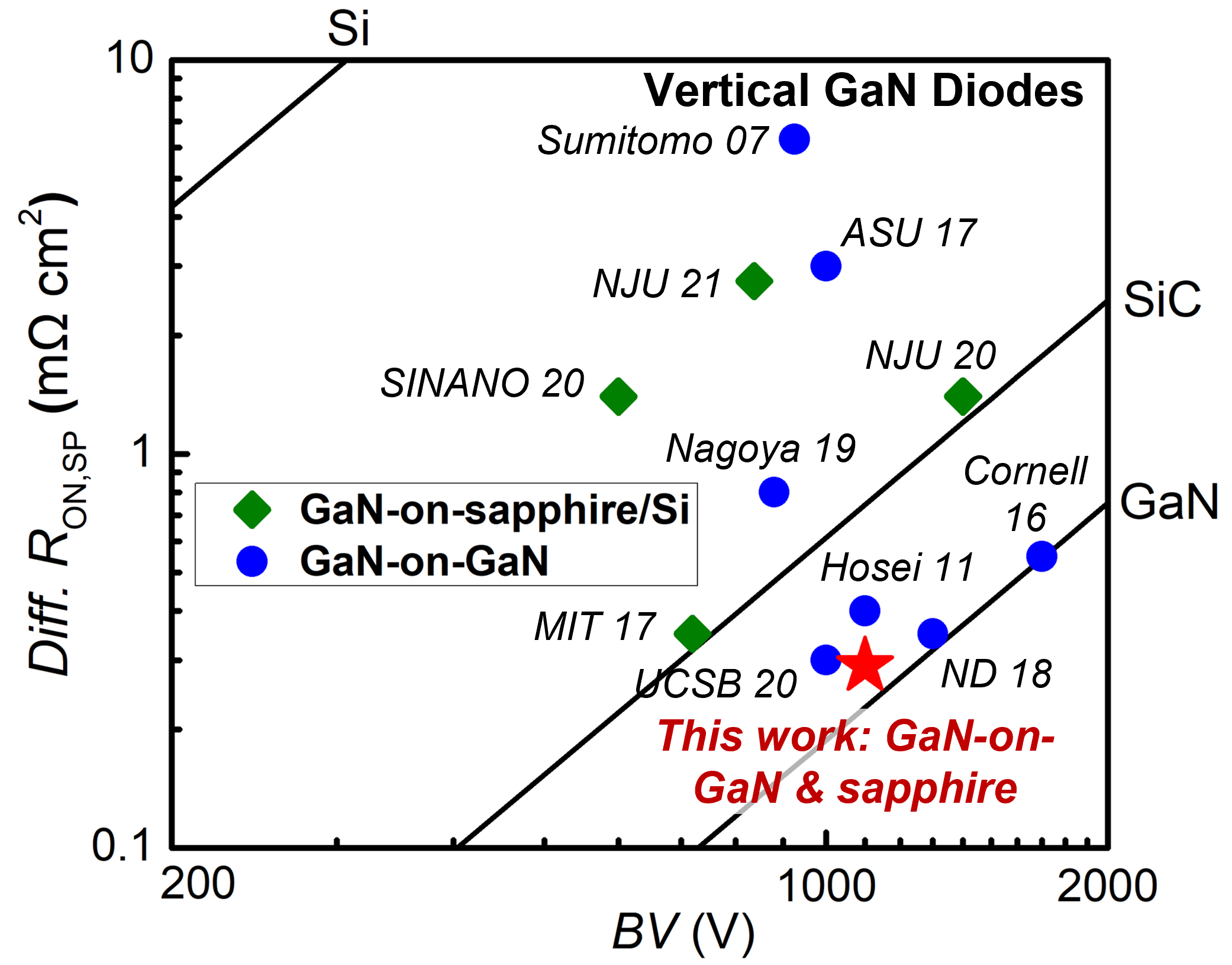
Fig.2 Differential specific on-resistance vs. breakdown voltage benchmark
Acknowledgement: Office of Naval Research (ONR), Grant N00014-
