


LIBRARY
Design Considerations of a Fast 0-Ω Gate-Drive Circuit for 1.2 kV SiC JFET Devices in Phase-Leg Configuration
Year: 2009
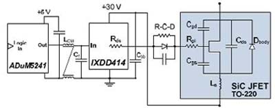
Fig. 1. Proposed gate-drive circuit for the SiC JFET.
The main component of the proposed gate-drive circuit (Fig. 1) is the IXYS gate driver IC IXDD414, which sources a maximum output current of 14 A and is among the fastest speed achievable for this power level and device based on reported data. To push the switching speed there is no gate resistor as observed in the circuit and the only resistance is provided by the output impedance of IXDD414 (~0.5 ω) and the internal gate resistance of the JFET. The R-C-D network is only used to compensate for the varying pinch-off and breakdown voltages of present JFETs but not to slow down the device switching. To provide control signal isolation, an Analog Device ADuM5241 integrated dc-dc converter is used, which has a common-mode transient immunity (CMTI) of 25 V/ns, and in addition CM chokes are added on both input / output sides to improve the CMTI.
The double-pulse tester used to evaluate the gate-drive circuit has a rating of 600 V dc and 10 A peak, and uses a 1 mH load inductor. The freewheeling diode is a 1.2 kV, 20 A SiC Schottky barrier diode (SBD) for fast switching compatibility. Regarding the PCB construction, the dc bus is built using planar structure which helps to minimize stray inductances, and is supported by big aluminum electrolytic capacitors to provide enough transient currents, and many film and ceramic capacitors with minimum equivalent series resistance (ESR) placed in maximum proximity to the SBD-JFET pair to provide sufficient bypass for the high frequency ringing current. Similar strategy is applied to the gate drive power supply (GDPS) as well. Besides, the CMTI of the GDPS is ensured by a HV-reinforced isolated dc-dc power supply Traco THB3-2423 with a minimized input-output capacitance of only 7 pF. Furthermore, the load inductor must be constructed with minimum equivalent parallel capacitance (EPC) as the energy stored in it would contribute to the JFET current overshoot during turn-on.
As the experiment turns out, the careful selection of ultra-fast gate drive circuit components together with the considerate PCB layout design leads to a turn-on time of 16 ns and turn-off time of 30 ns for the JFET under study when switching 600 V and 6 A, achieving a corresponding dv/dt of 60 V/ns and di/dt of 3 A/ns (Fig. 2).
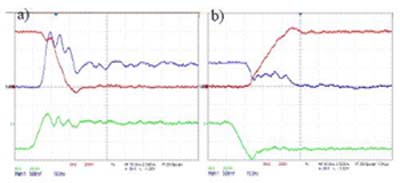
Fig. 2. Turn-on (a) and turn-off (b) switching transients at 600 V dc and 6 A inductive load current. Waveforms shown at 10 ns/div are: IDS 5 A/div (blue), VDS 200 V/div (red), and VGS 20 V/div (green).
