


LIBRARY
Experimental Parametric Study of the Parasitic Inductance Influence on MOSFET Switching Characteristics
Year: 2010
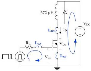
Fig. 1. Double-pulse tester for the parametric study.
The parametric study on the parasitic inductances is conducted on a double-pulse tester and the objects to be studied are narrowed down to three most critical parameters, namely the gate loop inductance LGS, the main switching loop inductance LDS, and the common source inductance LSS, as shown in Fig.1. These inductances are controlled independently, and, as they are increased gradually, the different switching waveforms of the power MOSFET are compared to show the respective effects of these inductances on the device switching loss, voltage and current stresses, and EMI emission.
The study shows that LGS tends to cause oscillation in the gate voltage VGS, but has only minor influence on the main switching waveforms such as the drain-source voltage VDS and drain current ID of the MOSFET. LDS would cause severe ringing in both VDS and ID, and also affect VGS greatly through the Miller capacitance. It also turns out that the parasitic ringing can cause increasing device stresses and EMI radiation, but hardly contributes to the switching loss. LSS, on the other hand, will greatly increase the switching loss due to its negative-feedback effect (Fig. 2 and Fig. 3).
Based on the study results, a design rule-of-thumb is to put the first priority on reducing LDS by placing the MOSFET and the freewheeling diode as close electrically as possible, and putting more low ESL bypass capacitors properly between bus rails to reduce the loop. LGS needs to be reduced as well but may come secondly. LSS should also be minimized to avoid increased switching loss.
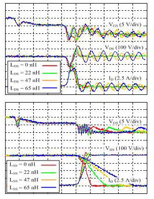
Fig. 2. Influences of LDS and LSS on the turn-off switching waveforms of a power MOSFET.
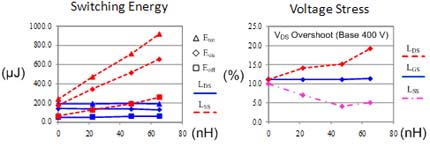
Fig. 3. Influences of different parasitic inductances on the switching energies and stresses of a power MOSFET (400 V, 10 A switching condition).
