LIBRARY
Modeling, Simulation and Design of a Very-High-Frequency Dual-Active-Bridge Converter
Beside the power device design and manufacturing issues, the main technological challenges in these applications are related to the effects of high dv/dt, high di/dt, and high-frequency losses on the converter operation and control, passive components and layout, as well as electromagnetic and thermo-mechanical integration. It is conjectured that the challenges remain similar at lower power applications if dv/dt and di/dt remain similar and switching frequency is proportionally increased, e.g. in a 600 V, 10 kW DAB switching at 500 kHz that could be implemented with 1.2 kV, 33 A, SiC MOSFET/JBS modules.
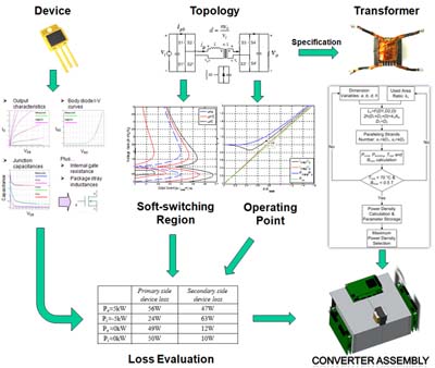
In order to study the DAB design issues and limitations when operated at very high switching frequencies, and to evaluate the conjectured scalability of the approach, this paper presents the simulation-based analysis and design of an initial prototype utilizing Si CoolMOS and SiC schottky devices in a 300 V, 5 kW, DAB converter switching at 500 kHz. The converter is designed by using simplified model for behavioral analysis and using simulation for verification and device stress estimation. First, the simplest model using ideal switches is utilized to evaluate the design specifications and size the passive components. The switch ratings are estimated for the device selection. Then a key parasitic - MOSFET junction capacitor - is added to the switch model to study an important feature of the converter - zero voltage switching (ZVS). The converter usually operates under ZVS at full load and is hard-switched at certain light load condition, which is usually not acceptable for the very-high-frequency applications. ZVS operating region is maximized by the newly proposed adjustments to the modulation scheme. Simulation with more detailed device models is then carried out to verify the analysis and to study how other non-ideal behavior of the devices affects the converter operation. Switching loss at 500 kHz is a major part of the total loss. Because the converter operation is quite different under different load conditions, the estimation of the worst case losses is very hard and must rely on detailed and extensive simulations.


