LIBRARY
Investigation of 1.2 kV SiC MOSFET for High Frequency High Power Applications
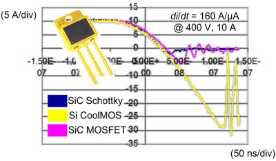
In order to investigate the performance of SiC MOSFET in high switching frequency application, a 1200 V SiC MOSFET with 4.1 x 4.1 mm2 die size has been fully characterized in both its static and switching performances. The device limitations in high switching frequency operation has also been analyzed and summarized. Compared with a state-of-the-art 600 V Si CoolMOS, the on-resistance of SiC MOSFET is more than 2 times smaller at room temperature and more than 4 times smaller at 150°C. Generally, the practical bottleneck of a high-frequency power converter is the power loss and the junction temperature. The low on-resistance can save the conduction loss and help the high-frequency operation to some extent. On the other hand, the critical device performance for ZVS operation is its body diode reverse recovery time Trr. The Trr of SiC MOSFET is comparable to that of SiC Schottky diode with the same voltage rating - less than 50 ns at 200 A/µs, and three times less than that of Si CoolMOS with ultra fast reverse recovery body diode (Fig. 1).
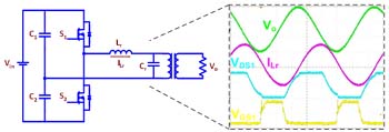
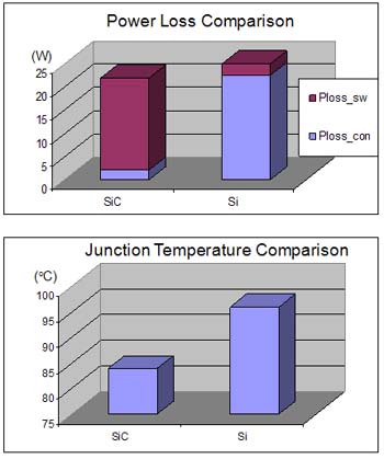
The SiC MOSFET under study has also been applied in a half-bridge parallel resonant converter (PRC). Fig. 2 shows the key waveforms of the SiC PRC operating at 1 MHz and 1 kW. Same PRC has also been operated with Si CoolMOS for device comparison purposes. As it turned out, SiC MOSFET had an obvious advantage on conduction loss due to its low on-resistance, but also suffered from higher switching losses compared with Si CoolMOS probably due to its higher output junction capacitance. However, the overall power loss of SiC PRC is still 10% smaller and the estimated device junction temperature is around 90% compared with Si technology (Fig. 3).
