LIBRARY
Investigation of Post-etch Copper Residue on DBC Substrates
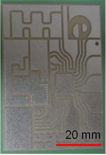
Electrolytic metal migration is a famous phenomenon which causes failure in microelectronic devices. This failure mechanism results in dendritic growths which bridge the electrode spacing between adjacent conductors on an insulating substrate and produce electrical failure. Therefore, it is very important to investigate what is going on at the surface of DBC alumina with copper residue leaving on it due to etching. Would any copper dendrites be formed between electrodes as our previous work on silver migration.
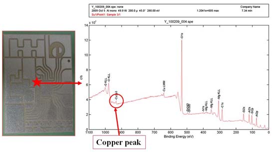
A comprehensive study of the influence of post-etched copper is carried out in CPES. Based on the analysis, a XPS result of commercial DBC with patterns is proposed shown in Fig.2. Copper peaks can also be located in the figure. The atomic concentration of copper is from 0.5%~0.7% which is consistent with that on the surface of DBC alumina patterned by our group. So it is indicated that copper residue on DBC surface during etching patterns is not a unique problem in our group. I have to say that it is very common issue in the industry. However, it seems like few people had reported this issue on DBC before. It may be caused by the amount of copper residue which might be too small to make the DBC alumina surface conductive at room temperature. But it is likely to be distinct in the high temperature application due to the lower resistivity and lower activation energy at high temperature.
