LIBRARY
Pressure-Assisted Sintering of Nanoscale Silver Paste
Solder alloys are routinely used for die-attachment and interconnection (for non-wirebond packaging). While they are relatively easy to use, they have low thermal conductivities and are susceptible to fatigue failure. Their low melting points limit the maximum operating temperature of the modules. Because the joint is formed by the solder reflowing process, the operating temperature of the joint can only approach the melting point. Even the high-temperature solder materials (high-Pb and Au-based) will be operating close to their melting points between 250 and 350°C. In addition, concerns about the health hazard posed by lead combined with the European RoHS directive coming into effect has led to the search for Pb-free alternatives, even with exemptions in place for some critical applications such as automotives and high-temperature systems. A metal or metal alloy that combines relatively low processing temperature and high-temperature capability is obviously a better choice.
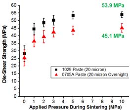
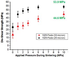
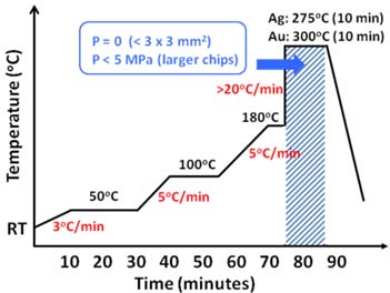
A nanosilver paste that can be used as a lead-free die-attachment has been developed. Follow the designed heating profile, Fig. 1, nanoscale silver paste can be fired at temperatures below 300°C and is capable of high temperature operation. The joint that is formed after sintering contains sub-micrometer to micrometer-scale pores that are randomly distributed in the microstructure. This type of microstructure gives a very low elastic modulus, 9 GPa, that is substantially lower than those of bulk silver and high-temperature solder alloys while the CTE is comparable to that of bulk silver. Its electrical and thermal conductivities are around five times higher than those of solder alloys. Typical die-shear strength of around 30 MPa can be obtained at 300°C or lower firing temperature at a relatively short peak temperature dwell time of 10 minutes and can be increased further by a higher firing temperature and/or the application of a small amount of pressure.
