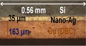
Fig. 1. Cross-Sections of Samples under Optical Microscopy.
The low-temperature joining technique (LTJT) by silver sintering is emerging as a high-reliability die-attach solution for power electronics modules of 175°C junction temperature. There is a great need to develop thermo-mechanical models of the LTJT modules for reliability prediction. However, lack of experimental studies on the mechanical properties of the sintered silver die-attach layer limits the modeling work. This study is an experimental effort to determine the residual stresses in large-area chip assemblies made by LTJT with nanosilver sintering; and, for comparison, residual stresses in soldered large-chip assemblies with lead-free solders of SAC 305 and SN100C are also measured. Silicon wafers of 0.5 mm thickness were diced into 10 mm x 10 mm samples. Direct-bond-copper (DBC) and copper with dimensions of 15 mm 15 mm 0.8 mm were used as substrates. LTJT bonding was carried out at 275°C under 3 MPa pressures; while soldering was done in a vacuum reflowing oven to reduce voiding. Bonding qualities were examined by an X-ray imaging tool and by cross-sectional scanning electron microscopy (SEM). Residual stresses in the chip-on-substrate assemblies were determined by measuring bending curvatures of the bonded structures. The bending curvatures were measured in an in-house optical setup based on the widely used thin-film stress measurement technique. From the measured bending curvatures and the mechanical properties of the constituent materials, residual stresses were calculated. Effect of temperature cycling on the residual stresses was also investigated. The chip assemblies were cycled between 40°C and 125°C and the changes in their bending curvatures were measured. Residual stresses were found to decrease with temperature cycling, which might be due to stress relaxation from creep or crack formation in the die-attach materials. Finally, microstructure evolution of the die-attach materials after hundreds of temperature cycles are presented.
The thickness of Bondline was checked by cutting of cross-section. The samples were observed under optical microscopy. Samples were, also, observed by using technique of X-ray (NordsonDage, Inc.). The area of voids is Less than 3% of the total die-attached area (exclude the area of spacer).
Due to relaxation of materials, residual stress inside Silicon of solder sample decreased after thermal cycling. Moreover, results of residual stress also shows that thickness of bondlines does not have obvious effect on the residual stress among samples with Solder SAC305 and SN100C. An advantage of nano-Ag paste should be pointed out: without using spacer, samples with nano-silver save die-attached area.
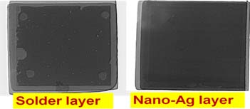
Fig. 2. X-ray pictures of samples.

Fig. 3. Residual Stress inside the Silicon Chip.


