


LIBRARY
Design Optimization of Non-uniform Flux LTCC Inductor Substrate for 3D Integrated POL
Year: 2011
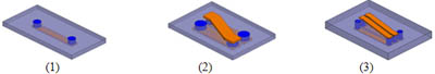
Fig. 1. LTCC lateral flux inductor. (1) 1-turn structure (N=1); (2) 2-turn structure (N=2); (3) 3-turn structure (N=3).
This LTCC magnetic material also has very non-linear permeability, which makes this problem even more unconventional and complicate. A inductor model was proposed by CPES to calculate inductance and core loss for these LTCCC inductor by dividing disc core into many concentric rings. Based on proposed inductor model, inductor footprint, volume and loss can be predicted and considered together to optimize the low profile LTCC inductor design. Fig.2 shows design curves for LTCC planar inductor. Fig.2(a) shows the impact of inductor footprint on inductor volume with give inductance value (L=300nH). it can be seen that 1) increasing turn number can reduce inductance volume. 2) there is an optimal footprint to give minimal inductor volume. Fig.2(b) shows the impact of inductor footprint on inductor loss with give inductance value (L=300nH). It can be seen that 1) increasing turn number will increase inductor total loss 2) when footprint is small, increasing footprint will reduce inductor loss, but after some point, further increasing footprint will not impact inductor loss too much. According to Fig.2, it can be seen that there is a footprint region to achieve small inductor volume and loss at the same time. For this case, the preferred footprint region should be from 50mm2 to 100mm2.
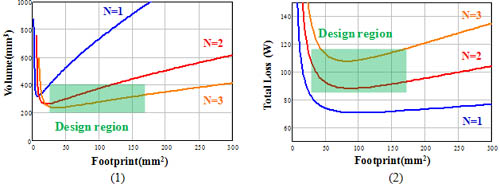
Fig. 2. Design curves for LTCC lateral flux inductor.
