


LIBRARY
Large-Area Chip Attachment by Sintering Nanosilver Paste: Nondestructive Characterization by X-ray Imaging and Curvature Measurements
Year: 2011
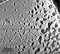
Fig. 1. X-ray reconstructed image of sintered micron-sized silver laye r in a commercial module, which shows the initial silver particles in the micrometer scale and significant numbers of voids and cracks are present in significant numbers.
This study focused on the use of nanoscale silver paste as the attachment material, which can be sintered at relatively low temperature and pressure. Contrast to the traditional press-aided sintering, an improved attachment technique is carried out, which can lower the temperature and time during the hot-press stage. With 3MPa pressure at 180°C for 5 minutes, the assembly can then sinter at 275°C without pressure. Test results on the attached samples showed that no detectable voids or cracks were found in the sintered silver layer and the device appeared to be strongly bonded when a measurable curvature was obtained.
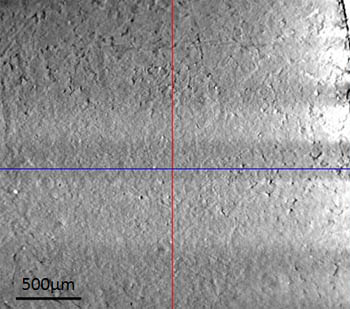
Fig. 2. Reconstructed x-ray image of the sintered nanoscale silver paste layer, which is generally uniform with only a few tiny cracks and pinholes possibly present.
