


LIBRARY
Compensation of DC-Link Oscillation in Single-Phase to Single-Phase VSC/CSC and Power Density Comparison
Year: 2012
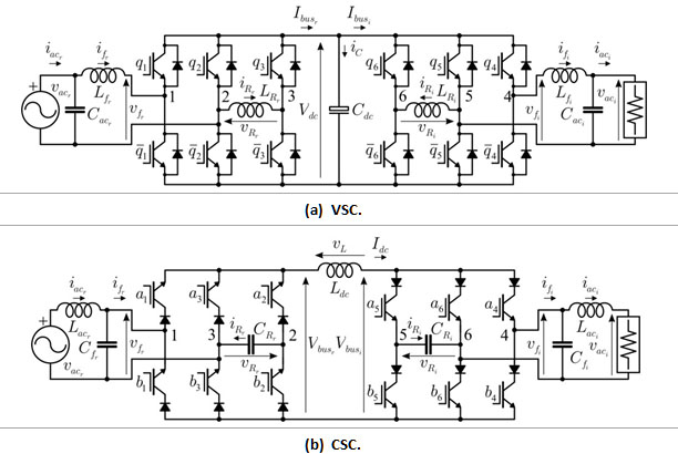
Fig. 1. Proposed single-phase to single-phase converters with oscillating power compensation.
In Fig. 2 are a comparison and simulation results for the converters. The volume comparison results are shown in Fig. 2(a). The inductor size is mainly determined by maximum flux density and loss. Different ripple energy and supply frequency applications will lead to different materials to achieve minimum volume. In terms of energy density, the film capacitor is more compact for low ripple energy, high-frequency applications. Otherwise, an aluminum capacitor would be better. For most of the application range, the inductive ripple energy storage method is bulkier and heavier than capacitive energy storage.
For the VSC, shown in Fig. 2(b), the system operates at 1kW with a Vdc*=320V, and 110V/50Hz and 220V/60Hz for the rectifier and inverter sides, respectively. For the CSC, shown in Fig. 2(c), the system also operates at 1kW with an Idc*=14A, and 220V/60Hz and 110V/50Hz for the rectifier and inverter side, respectively. In Figs. 2(b) and 2(c), (top), are shown the Vdc*/Idc* for the VSC/CSC using a bus capacitor of 40µF (VSC) and a bus inductor of 30mH (CSC). With the DC capacitor and inductor values used, a DC ripple of 3.77V (VSC) and 0.22A (CSC) were reached. To obtain the same ripple seen for the proposed system, it would be necessary a capacitor Cdc of 2,200µF (VSC) and a inductor Ldc of 1,400mH (CSC) in a conventional converter. Thus it was possible to achieve a reduction of 55 in the DC capacitor of the VSC and 46.67 in the DC inductor of the CSC. In Figs. 2(b) and 2(c), (bottom), are shown the waveforms of the signals in the AC side of the VSC and CSC, respectively. It is possible to observe that it was reached the unity power factor for the current iacr provided for the grid and a good waveform for the Vaci.
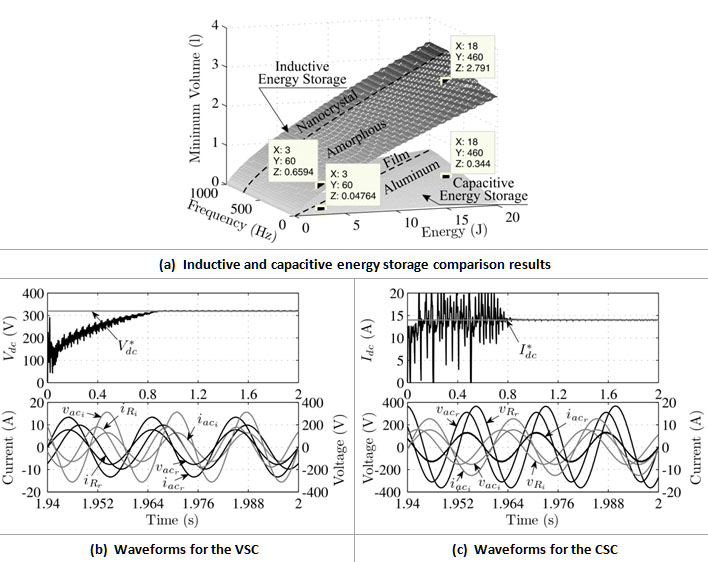
Fig. 2. Comparison and simulation results; (b) and (c) (top) are for the DC sides and (bottom) are for the AC sides.
