


LIBRARY
An Update on Recent Advances in Nanosilver Paste for Packaging Power Semiconductor Devices
Year: 2013
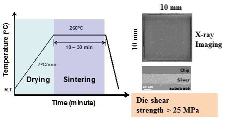
Fig. 1. Formulated a new nanosilver paste with simpler heating profile for pressure-less bonding of large-area chips.
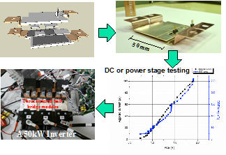
Fig. 2. Developed a planar, low-profile, double-side cooled, nanosilver-bonded power module.
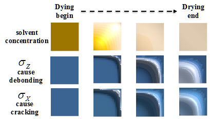
Fig. 3. Built a theoretical model for nanosilver chip bonding process to gain better understanding on defect formation in sintered bond-line.
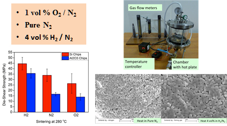
Fig. 4. Studied the effect of sintering atmosphere on chip bonding strength with nanosilver on bare copper.
