


LIBRARY
High Switching Frequency, High Efficiency, Modularized 3-level Neutral Point Clamped Phase Leg Building Block
Year: 2013
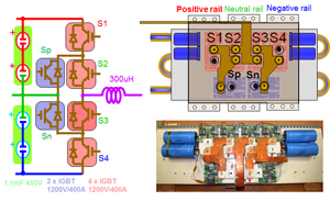
Fig. 1. 3-level NPC phase leg structure and layout.
The phase leg structure and layout are shown in Fig.1. Each phase leg has four main switches, which are 1200V/400A single IGBT module. Two clamping devices are in the same rating. DC link capacitors are evenly distributed on each phase leg to support the DC link voltage. All the interconnection for devices and phase leg are implemented by laminated bus bar, which can effectively reduce the loop parasitic inductance. The optimized layout design reduces loop inductance and can therefore improve switching performance.
The switching loop in a 3-level phase leg can be categorized into two types as shown in Fig.2. The switching loop for the outer switch is shorter with 2 modules and 1 connection. On the contrary, the inner switch loop is longer with 4 modules and 3 connections, resulting in a larger loop parasitic inductance. The switching characteristics for the inner and outer switch loop are therefore different. The gate resistor for the inner and outer switch should be selected accordingly. The gate resistance is a key factor for switching performance optimization as it influences both the switching loss and stress. To achieve both a high switching frequency and a high efficiency, a gate resistor value should be small enough to minimize switching loss. But voltage and current stress will be inevitably increased. The tradeoff for loss and stress should be considered and treated differently for inner and outer switch for an optimum switching characteristic. Based on the experimental result, the total loss for one line cycle can be calculated under a different operating condition. Fig.3 gives the total system loss for both the diode clamped NPC (DNPC) and the active clamped (ANPC) converter under a different power factor. The system efficiency is around 98% with a 20 kHz switching frequency.
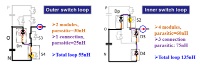
Fig. 2. Parasitic inductance with different switching loops.
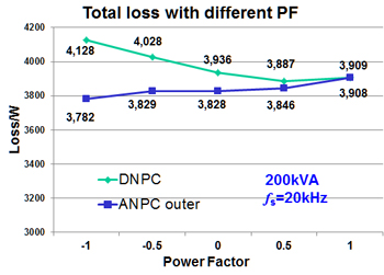
Fig. 3. Total system loss with different power factor for DNPC and ANPC phase leg.
