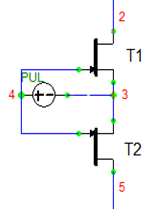
Fig. 1. Schematic representation of bidi-rectional switching GaN transistor. Nodes 2 and 5 are the drains of transistors T1 and T2 respectively. Node 3 connects the source of T1 and T2. Node 4 is the gate for T1 and T2.
Figure 1 shows the schematic representation of a bidirectional transistor consisting of two discrete switches. This circuit was realized with a commercially available 200V, 3A GaN HEMTs (EPC-2012) laid out on a PCB. The constituent transistors were fully characterized, then modeled using Statz' GaAs JFET model as a reference. Figure 2 demonstrates the accuracy of the model compared to experimental data. The model shows a very good correlation to the experimental results all the way up to 125°C.
Next, the bidirectional switch was simulated using the model developed for the con-stituent transistors, its output I-V compared to experimental results is detailed in Figure 3.
Finally, the bidirectional transistor was used to switch 100V at 3A with a switching speed of 21ns. In addition, it exhibited an on-state resistance of only 114m%uF057 and a blocking voltage of 200V in both polarities with the gate voltage equal to 0V!

Fig. 2. Model for EPC 2012 (solid lines) versus data () in the first quadrant at 25%uF0B0C and VG from 2 to 5V.

Fig. 3. Model for EPC 2012 (solid lines) versus data () in the third quadrant at 125C and gate voltages from 2V to 5V.
