LIBRARY
Analytical Loss Model of High Voltage GaN HEMT in Cascode Configuration

One popular analytical loss model is the piecewise linear model, which enables simple and rapid estimation of switching loss. However, the main drawback is that it doesn't consider the parasitic inductors and nonlinearity of the junction capacitors of the device. Therefore, the result normally doesn't match the experimental results very well, especially in high frequency applica-tions.
The other popular way to estimate switching loss of a high voltage device is based on measurement. For example, turn on energy (Eon) and turn off energy (Eoff) can be calculated based on double-pulse-test waveforms. However, the current probes introduce a substantial delay in the waveforms, typically a few nanoseconds. This delay can be estimated and proper correction introduced, but for fast switching circuits (capable of traversing from rail to rail in few nanoseconds) the error will remain huge. On the other hand, the Eon / Eoff obtained from the double-pulse-test only applies to certain test conditions including the PCB layout parasitic inductors, the capability of the driver and the characteristic of the free-wheeling diode etc.
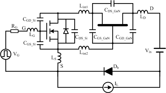
This paper analyzes the switching loss of the high voltage GaN HEMT in cascode configuration with a novel analytical model. The proposed model considers the package including the PCB layout parasitic inductors, the nonlinearity of the junction capacitors and the transconductance of the cascode GaN transistor. The switching loss is obtained by solving the equivalent circuits during the switching transition. The model is easy to understand and provides a deep insight into the switching process.
To analyze the switching loss, a simple Buck converter is used as an example. A freewheeling diode is used as the bottom switch and the parameters of the diode represent whatever electric characters in the real case. The inductor current is treated as a current source during the transition time. The final circuit model used to analyze the cascode GaN transistor switching loss is shown in Fig. 1. Actually, the simplified equivalent circuit in Fig. 5 is also suitable for other bridge configuration based topologies, such as Boost, Buck-Boost etc., to analyze the device behaviors during transition period.


