LIBRARY
Avalanche Breakdown Design Parameters in GaN

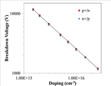
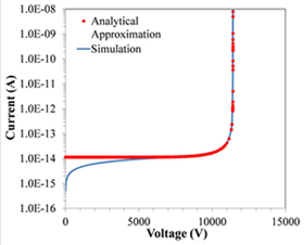
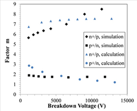
Next, the shapes of the avalanche breakdown I-Vs of the GaN obtained from numerical simulations were examined. The avalanche I-V was found to be sharper for GaN n /p junctions than p /n junctions with the same doping. Similarly to silicon, the sharpness of the GaN avalanche I-V can be measured by the factor m as in the analytical approximation =I0/(1-(V/BV)m) , where I0 is the pre-avalanche leakage current. For silicon, m is different for different BVs, although it has been known to be 6 for p /n junctions and 4 for n /p junctions for simplification. The m is also related to the BV of BJTs in terms of BVcbo/BVceo= (1 β)1/n , and has been extracted for SiC BJTs to be around 8 to 10. We have extracted the m value as a function of BV for GaN fitting the GaN avalanche I-Vs from simulations with the analytical approximation (see Fig. 2), and got m increasing from 5.7 to 8.5 in the BV range of 1.2kV to 12kV for GaN n /p junction; and m decreasing from 1.9 to 1.8 for GaN p /n junction (see Fig. 3). We also obtained m by calculating the ionization integral numerically as a complementary method, and received similar results (see Fig. 3). The slight difference may be attributed to the fact that the ionization integration method lacks the field modification by the carriers in transient. Because the higher m yields a sharper avalanche I-V, GaN n /p junction is projected to be a better choice for the main voltage blocking junction in GaN power devices.


