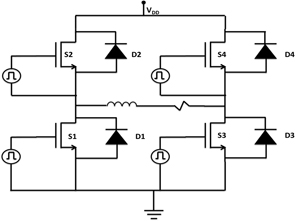
Fig. 1. Full bridge inverter circuit topology.
Figure 1 shows the schematic of the full bridge invertor circuit topology used for SPICE simulations. It consists of four switches (S1-S4) and four anti-parallel diodes (D1-D4). This type of circuit is typically used to drive inductive loads such as motor drives, represented here using an inductor with a series resistance. The switches are typically driven through a gate drive circuit, simulated here using a pulsed voltage source. The SPICE simulation is performed for an all SiC and all GaN circuit and compared with an all Si based circuit. For the SiC based circuit, SPICE models for the 1200V SiC DMOSFET from Cree Inc. were used. A SiC Schottky model developed by us for a 600V SiCED SiC Schottky was used for the antiparallel diode. For the GaN based circuit, a SPICE model for a lateral 200V GaN HEMT from EPC was used, and a GaN Schottky model developed by us was used for the antiparallel diode. The GaN HEMT was simulated as three devices in series to simulate the increased conduction losses for an equivalent 600V device. Bus voltage of 600V was used and the load was adjusted to get a load current of 10A. A duty cycle of 50% was used for the gate drive voltage sources and a dead time was introduced between the voltage sources in the same branch so as not to short the bus voltage to ground due to the finite rise and fall times of the voltage sources. The gate voltage for the SiC MOSFET was switched from 0V to 20V and the gate voltage for the GaN HEMT was switched from 0V to 5V, since the gate turns on beyond 5V.
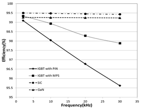
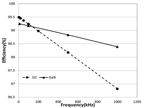
The efficiency of the circuit was measured by calculating all the losses in the switches, diodes and gate drives. The efficiency of the GaN is higher at higher frequencies than the SiC and drops off less slowly compared to the SiC. This performance improvement in the GaN at high frequency is largely due to the lateral structure of the GaN device. SiC MOSFET is a vertical device and hence has larger gate-drain overlap capacitances when compared to a lateral device.

Fig. 2. Efficiency comparison at low frequencies.

Fig. 3. Efficiency comparison at high frequencies.
