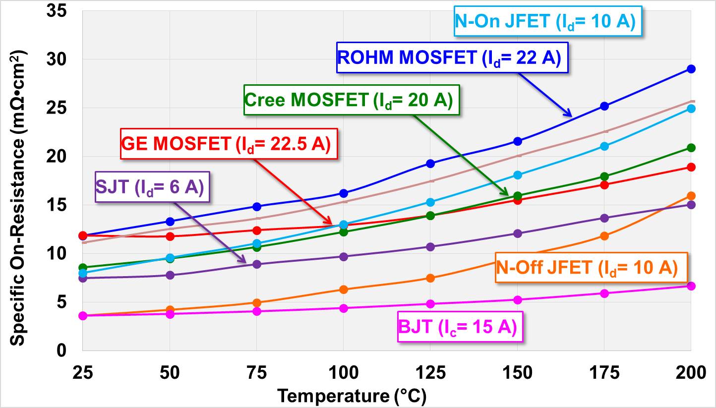
Fig. 1. Specific on-resistance using die area versus temperature.
A significant effort has been devoted to characterizing the numerous Silicon Carbide (SiC) power semiconductor devices under development. Of these devices, the SiC MOSFET has re-ceived significant attention up to now given its maturity, relative ease of commercialization, and simple driving scheme. While recent studies have shown that the gate-oxide of the SiC MOSFETs is reliable beyond 200 °C, which remained one of the major barriers of this device until now, oxide-free structures such as the BJT, and normally-on and normally-off JFETs have been pursued as well. Since high-temperature operation is one of the major advantages offered by SiC over Si, it is of great interest to evaluate the performance of these devices under extreme temperature conditions.
The on-resistances of each device were measured using a curve tracer. It is important to look at the specific on-resistances of the devices since for a given breakdown voltage the smaller the die size the larger the resistance. In this case, this figure was obtained by multiplying the measured on-resistance values by their respective die area.

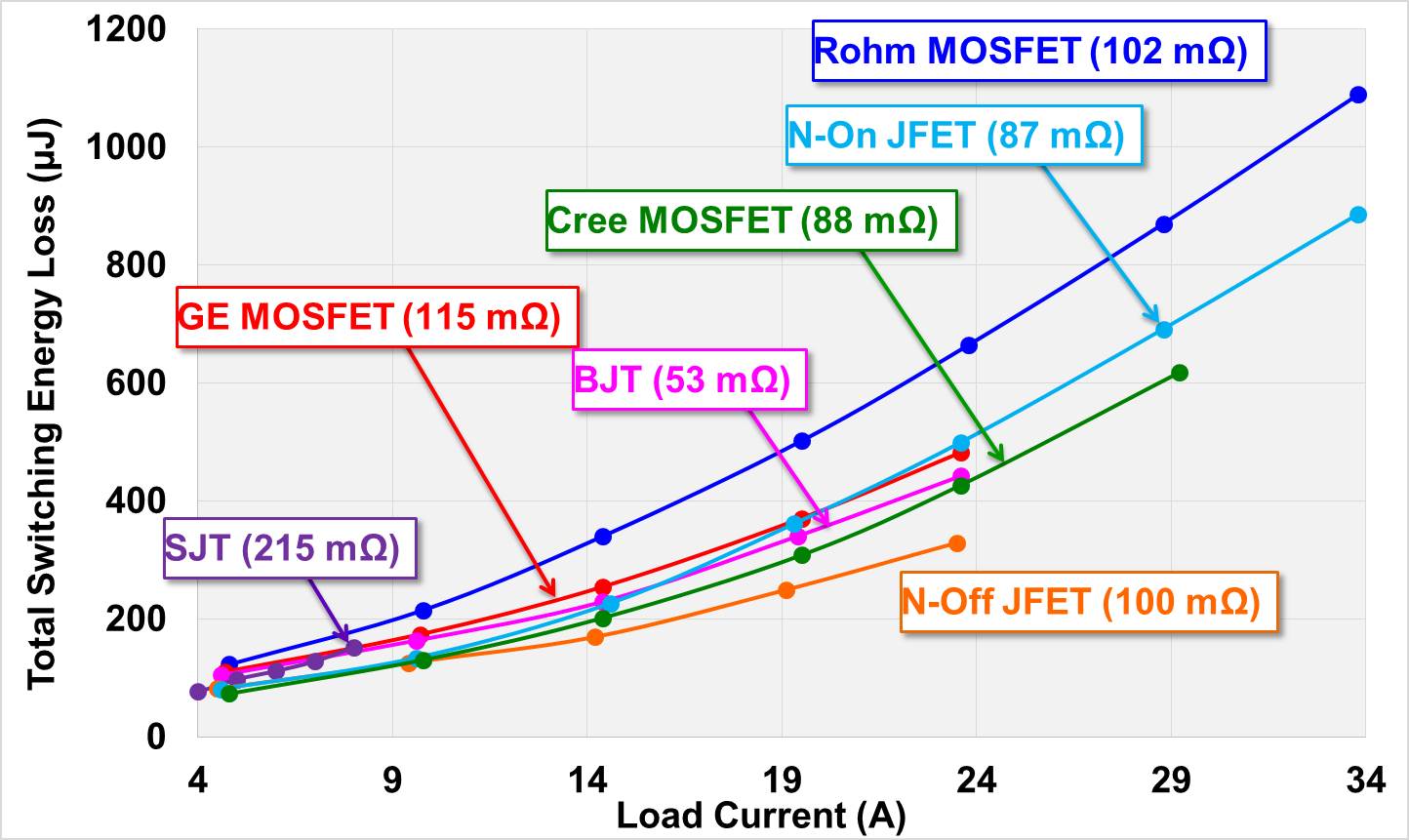
Fig. 2. Total switching energy loss versus load current.
