LIBRARY
1200V Bi-Directional Si DMOS IGBT Fabricated with Fusion Wafer Bonding
In this paper, we report results demonstrating that a flat and clean surface is the key requirement for a hydrophobic bonding process producing an electrically transparent junction. Wafers can receive final polish and scrub clean after being thinned down to a thickness of 150µm by mounting them onto glass carriers using a benzocyclobutene based resin (BCB). After diffusion groove fabrication, surface cleaning, and dilute HF treatment, the wafers are aligned back to back and then bonded with a slow ramp rate to 400°C. They must stay at 400°C for 24 hours under atmospheric vacuum and mechanical pressure. After bonding, the glass carriers delaminate from the bonded pair, since the BCB between silicon device wafers and the glass carrier wafers is degraded during the 400°C silicon bonding process.
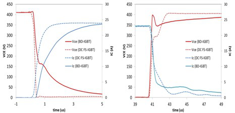
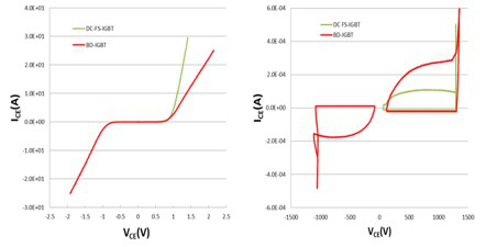
Static and dynamic measurement was performed using a Tektronix 371A curve tracer. The forward conduction and breakdown characteristics are shown in Figure 1. The forward voltage drop was measured at 2.2 V in the first quadrant and 1.9 V in the third quadrant at a current of 25 A, while the breakdown voltages were measured at 1400 V in the first quadrant and 1050 V in the third quadrant at a current of 500 µA. The testing result implies that a good electrically transparent bonding interface is achieved. For switching performance, the turn on and turn off characteristics at a current of 15 A are illustrated in Figure 2.
In summary, the bi-directional IGBT has been successfully fabricated and characterized. The electrical results demonstrate the feasibility of low temperature hydrophobic wafer bonding to achieve good static and dynamic performance.
