


LIBRARY
Package Influence on Switching Performance of SiC Modules
Year: 2015
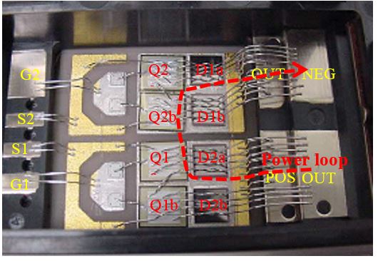
Fig. 1. Internal view of 1.2 kV / 100 A SiC module showing two 80 A SiC MOSFETs and two 50 A SiC JBS diode per switch.
The first is to model the parasitic as a DC resistance in series with the AC inductance; another way is to model the parasitic as an AC resistance in series with the AC inductance. In addition, the simulation frequency is usually set the same as the switching frequency. In this paper, the model is changed to be an AC resistance parallel with the combination of a DC resistance in series with the AC inductance. This model should present accurate dynamics for both low frequency and high frequency. Choosing the simulation frequency is also further discussed in the paper. The maximum element length of the mesh should be set to no larger than the skin depth of the simulated conductor.A tradeoff has to be made between the simulation time and the switching frequency for practical use. Simulation results using the conventional modeling method, and the proposed modeling method are compared with the experimental results. The proposed modeling method agrees with the experimental results. Once the accurate modeling method is concluded, the parasitics of five 1200 V SiC commercial modules are extracted to build the simulation schematic in LTspice. Fig. 2 shows three different half-bridge configurations. The same MOSFET and diode dice are used to fairly evaluate the switching performance of each module affected mainly by the package parasitics. The layout characteristics of each module are summarized and compared. Among them, the largest gate inductance is 101 nH. Current unbalance and self-turn-on issues are noticed and analyzed by looking into the internal switching performance.
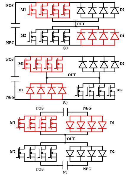
Fig. 2. Different half-bridge configurations.
