


LIBRARY
Characterization and enhancement of high voltage cascode GaN devices
Year: 2015
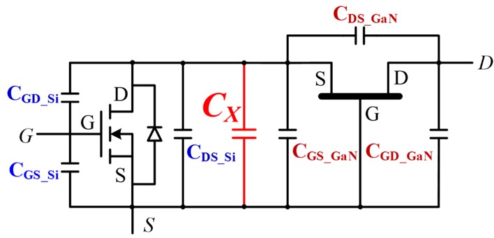
Fig. 1 Adding an extra capacitor to the cascode GaN switch.
For off-line applications, enhancement-mode (normally-off) and depletion-mode (normally-on) GaN switches are available. The depletion-mode switches usually have a lower on-resistance and a smaller junction capacitance than the enhancement-mode switches. They are, therefore deemed more attractive for applications that require high efficiency at a higher frequency. The depletion-mode GaN switch in series with a low voltage silicon MOSFET is also an appealing alternative. This configuration is known as cascode structure. In the cascode structure, the voltage distribution between GaN and Si MOSFET may result in the unwanted avalanche of the Si MOSFET as well as the internal switching loss for the depletion-mode GaN switch even when it is intended to operate under the soft-switching turn-on transition. A simple and effective way to solve the issues is to add an extra capacitor in parallel with a drain-source of Si MOSFET to compensate the capacitor charge mismatch as shown in Fig. 1. A parallel extra capacitor between the drain-source terminals of the Si MOSFET will not increase its driving loss, and the turn-off loss is still very small due to the merits of the cascode structure. This simple approach could enhance the switching performance of the cascode GaN switch. Moreover, this prevents the silicon MOSFET from reaching avalanche and improves the device reliability.
To demonstrate the advantages and explore the potential of the high voltage cascode GaN switch, a 5 MHz 180V/400V CRM boost converter is developed. To avoid device capacitor mismatch and the package parasitic inductance impact on switching performance, a chip-on-chip packaged cascode GaN integrated with an extra capacitor (800pF, 1mm*0.5mm* 0.5mm) is fabricated and applied in this converter. The prototype of the cascode GaN switch and the boost converter are shown in Fig. 2. The converter can achieve 98% efficiency and 1000 W/in3 power density at 600W output conditions.
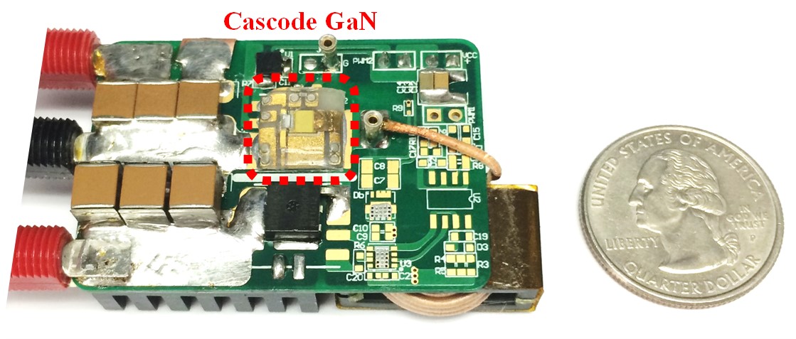
Fig. 2. Prototype of 5 MHz converter with cascode GaN switch
