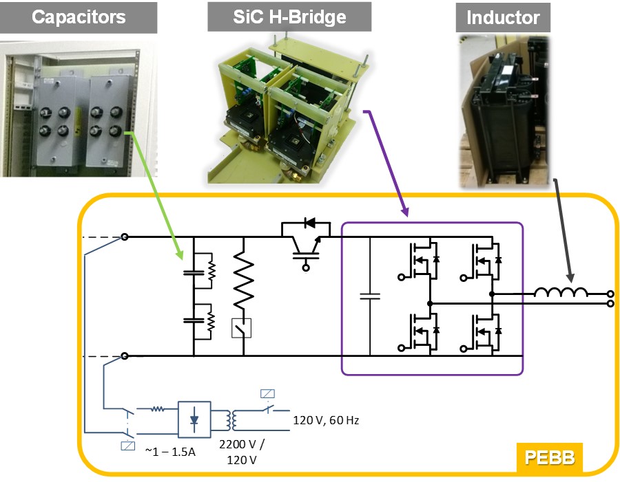
Fig. 1. PEBB with bulk capacitors, SiC H-bridge, and inductor
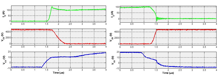
For this work, 10 kV, 120 A, all-SiC half-bridge modules were tested and simulated for use in 4 kV, 100 A power electronics building blocks (PEBBs), which are standard, multifunctional units that can replace specialized devices in order to simplify the design and reduce the cost of converter systems. This PEBB design consists of four 10 kV SiC modules in an H-bridge configuration (Fig. 1). Each module contains twelve parallel 10 kV SiC DMOSFETs, and six parallel 10 kV SiC junction barrier Schottky (JBS) diodes. Double-pulse tests (DPTs) were conducted on the 10 kV modules up to 4.7 kV and 100 A in order to evaluate their hard switching capabilities. The DPT results revealed fast switching of the modules, and minimal ringing and overshoot. A Saber model of the module was then compared to the experimental results, which showed sufficient agreement with the testing waveforms. This model was then used to simulate the PEBB operation.
The PEBB structure and layout are shown in Fig.1. In addition to the SiC H-bridge, each PEBB has two arm inductors, two series DC link capacitors, and a 6.5 kV IGBT for short circuit protection. The IGBT is always conducting unless the desaturation protection on the IGBT gate driver is triggered. This is meant to protect the H-bridge from the energy stored in the DC link capacitors. All the interconnections are implemented with a laminated bus bar, which can effec-tively reduce the loop parasitic inductance. The optimized layout design reduces loop induct-ance and can therefore improve switching performance.

Fig. 2. Turn on (left) and turn off (right) DPT waveforms at 4.7 kV and 100 A with the drain current (top), drain-source voltage (middle), and gate-source voltage (bottom) shown
