LIBRARY
Design of a High-Density, Diode-less 1.2 kV, 90 A SiC MOSFET Half-Bridge Power Module

In this work, a 1.2 kV, 90 A, diode-less SiC MOSFET half-bridge module was designed, fabricated and tested. A survey of packaging materials and technologies was conducted, and the selections were based on the tradeoff between cost and performance.
When designing the power module layout, several factors must be considered. In order to minimize parasitic inductances, the layout should be compact enough that the conduction paths are short. However, to successfully extract the heat from the module, sufficient space is needed between devices, and the substrate metallization and baseplate should be large enough to effec-tively spread the heat. There is hence a tradeoff between the electromagnetic and thermal per-formances. The optimal compromise between these characteristics was determined using AN-SYS Q3D and ePhysics.
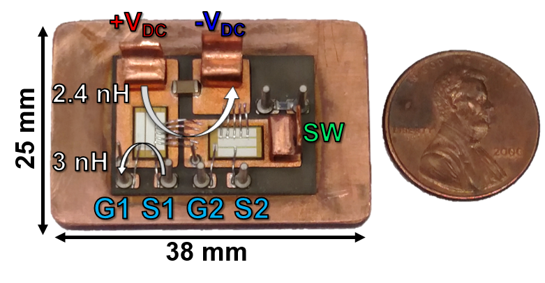
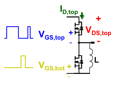
The designed module (Fig. 1) has low gate-loop and power-loop parasitic inductances of 3 and 2.4 nH, respectively, and has more than twice the power density (7.8 W/mm3) of similarly-rated commercial half-bridge modules. Double-pulse tests (DPT) performed on the fabricated power module at 800 V and 50 A revealed a total switching loss of 1.3 mJ, which is less than half that of similarly-rated commercial half-bridge modules. Additionally, the DPT waveforms (Fig. 2) showed a low voltage overshoot of less than 9% of the dc bus voltage. This small voltage overshoot can be attributed to the low power-loop parasitic inductance. The module also achieved a high dv/dt of nearly 60 V/ns. In the future, the module will be used in a boost con-verter in order to evaluate its performance under continuous operation.


