LIBRARY
Static and dynamic performance characterization of 3.3-kV 30A discrete SiC MOSFETs from Sumitomo Electric Industries

SiC semiconductors are in the early stages of their evolution, and, especially at higher volt-ages, they are not yet fully developed. However, device manufacturers are doing research and producing sample devices now that will finally lead to commercial SiC semiconductors. The ultimate goal of this paper is to characterize and compare four sample SiC MOSFETs at 3.3-kV 30A in a TO-247 full-mold package that includes a single die inside. The received samples have part numbers D10, D14, T10 and P12, and will be referred to with these names in figures and tables.
This paper characterizes and compares the room-temperature and high-temperature performances of the mentioned MOSFETs. A complete static and dynamic characterization is done on all devices at the temperatures 25°C, 100°C and 150°C, feeding the devices with their datasheet-recommended -5/ 15V gate-to-source voltage. The static characterization includes output characteristics, transfer characteristics, on-state resistances, threshold voltages and capacitance measurements. The dynamic characterization, on the other hand, includes double-pulse tests at the same temperatures at four different gate resistances to achieve loss variation according to the gate resistance for the devices. The switching losses are calculated and compared through these double-pulse tests.
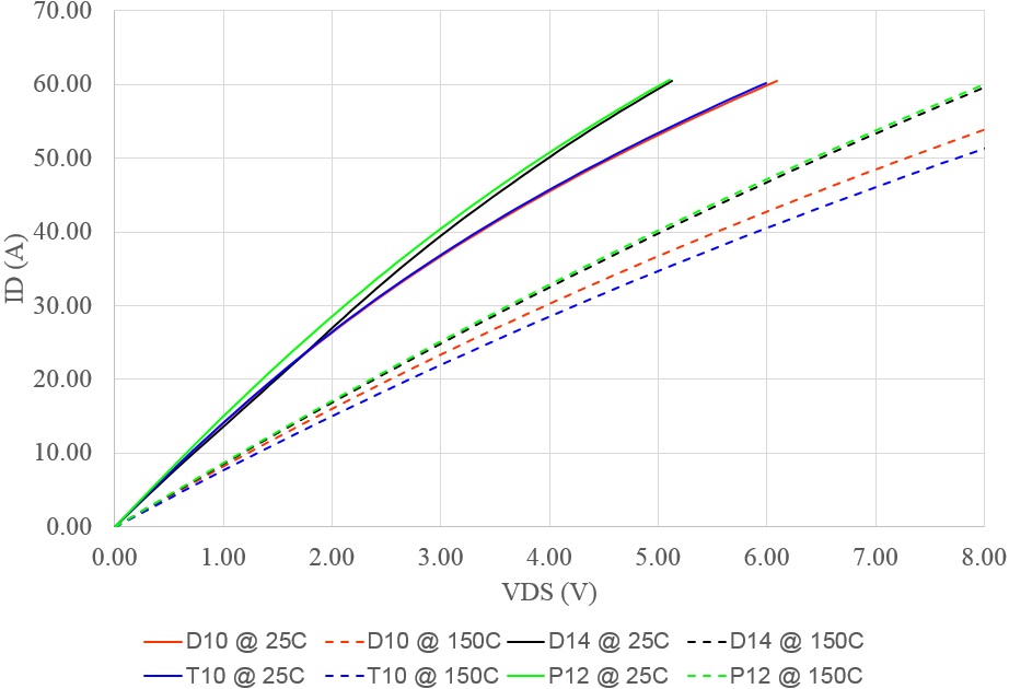
The output characteristics of the devices under test are shown in Fig. 1 at 25°C and 150°C. The results show that the MOSFETs D10 and T10 have a similar structure. In addition, the D14 and P12 devices show similar characteristics at both room temperature and high temperature.
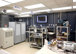
Fig. 2 shows the double-pulse test setup used to do the dynamic characterization. The capacitors are connected via busbar, an IGBT desaturation overcurrent protection is used for possible DUT failure protection, and the load inductor and the actual double-pulse tester PCB can be seen. The gate signal is optically isolated for safety considerations.


