


LIBRARY
Characterization and comparison of the latest generation of 900-V and 1.2-kV SiC MOSFETs
Year: 2016
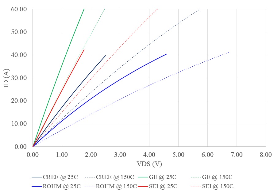
Fig. 1. Output characteristic of the devices under rec-ommended VGS in each case.
With the emergence of the newer generation SiC devices, the question that arises is how the performance of the new generation of devices from different manufacturers compare to each other. Thus this paper characterizes and compares the room-temperature and high-temperature performance of the latest generation of discrete 900-V and 1.2-kV SiC MOSFETs from four well-known manufacturers: CREE, ROHM, GE and Sumitomo Electric Industries (SEI). The Cree MOSFET is in a D2PAK package and the rest are packed in To-247 packaging.
A complete static and dynamic characterization is done on all devices at four different temperatures; 25°C, 100°C, 150°C and 200°C; feeding each device with the gate-to-source voltage recommended by the datasheets. The recommended gate-to-source voltages are -4/ 15V, -4/ 18V, -4/ 18V and -5/ 15V for CREE, ROHM, GE and SEI SiC MOSFETs, respectively.
The static characterization includes output characteristics, transfer characteristics, on-state resistance, threshold voltages and capacitance (Miller capacitance, input capacitance and output capacitance) measurements for all devices. The dynamic characterization, on the other hand, includes double-pulse tests at the same temperatures and adjusting the gate resistances to achieve the same switching speed on all devices. The switching losses are calculated and com-pared through these double-pulse tests.
The output characteristics of the devices at their corresponding recommended gate-to-source voltages and two temperatures, 25°C and 150°C, are shown in Fig. 1. It is clear that the GE device has the smallest on-state resistance, while the ROHM semiconductor has the highest. The double-pulse test setup used to test the devices up to 200°C is shown in Fig. 2. This setup includes the actual double-pulse tester, an IGBT desaturation protection board used to protect the setup from possible DUT failure, and a hot plate, which is used to heat the device up to the desired temperature.
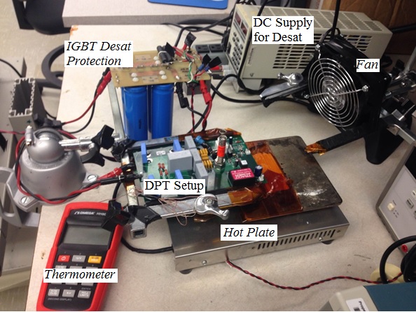
Fig. 2. High-temperature DPT setup.
