LIBRARY
Dynamic Sharing Between Paralleled SiC MOSFETs Caused by Threshold Voltage Mismatch

Parasitic inductances are introduced by package or layout that electrically connects bare dies. Lots of research focuses on dynamic sharing caused by asymmetric layout, which can be easily removed by a careful layout design. However, the existing methods to mitigate dynamic sharing origins from device mismatch are usually complex and expensive, which normally require separate gate drivers, complex current sensing and an active control circuit. This paper introduces a simple and passive method to reduce transient sharing caused by Vth mismatch.
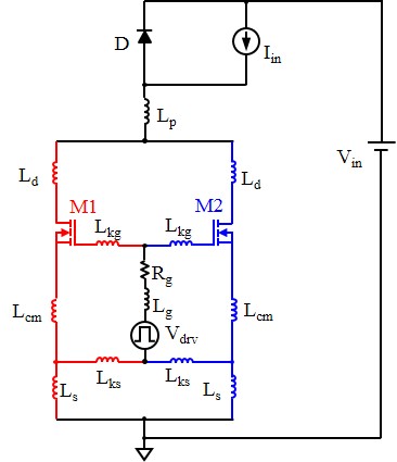
The equivalent circuit model considering all the parasitic inductances is shown in Fig. 1. The objective of this paper is to mitigate the imbalance caused by device mismatch. Symmetrical layout is employed in order to avoid the imbalance origins from an external package. Their influences on parallel dynamic performance are comprehensively investigated with regard to switching loss, voltage stress, and switching loss imbalance.
Influence of Lks and Ls on switching loss imbalance is shown in Fig. 2. According to the results, Lks and Ls can greatly reduce dynamic sharing between M1 and M2. Even though Ls will increase device voltage stress together with small power-loop inductance Lp, the voltage stress, as long as it is not super large and stays within the nH level, can be controlled within an acceptable range. Furthermore, switching loss is not sacrificed.


