


LIBRARY
Unified Equivalent Circuit Model and Optimal Design of V2-Controlled Buck Converters
Year: 2016
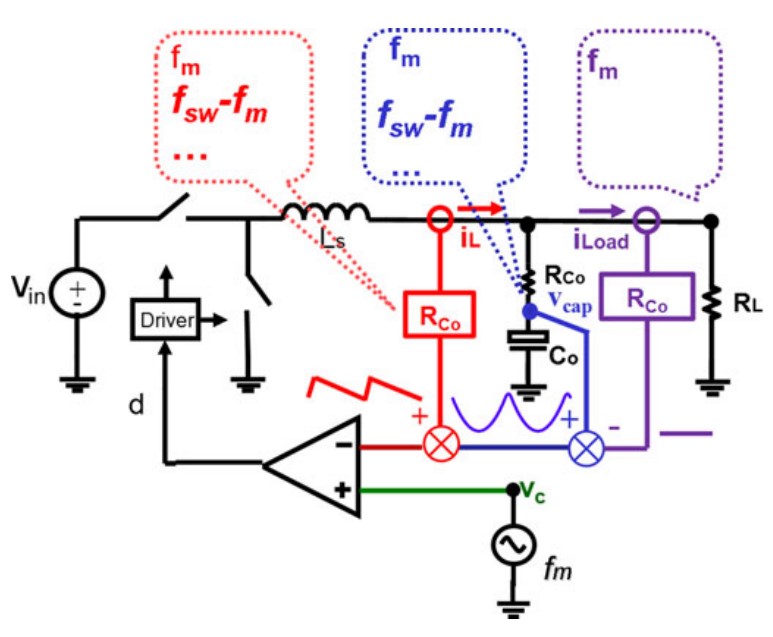
Fig. 1. Frequency spectrum of direct feedback loop of V2 control with three feedback paths
The analysis shows that the buck converter with V2 control can be regarded as a non-ideal voltage source. The methodology used to derive an equivalent circuit model to represent this non-ideal voltage source is to establish the connection between V2 control and current-mode control; as the equivalent circuit model of current-mode control is well established, the resulting equivalent circuit model is shown in Fig. 2. The non-ideal current source and non-ideal voltage source are virtually represented by the resonance between Ls and Ce and Le and Co, respectively. The damping factor of the double poles caused by the capacitor voltage sideband is determined by the damping resistance Rdamp, depending on the capacitor parameters.
Due to the low ESR of ceramic capacitors, when they are used V2 has stability limitations to be applied. Several methods have been proposed to address this issue; one is using enhanced V2 constant on-time control by adding current ramp information; the other method where adaptive voltage positioning is undesired is using the enhanced V2 constant on-time control with a high-pass filter after current sensing; the third method is sensing the capacitor current. The complete equivalent circuit model for these three methods is also derived in this work and shown in Fig. 3. A unified equivalent circuit model for V2 control is also proposed, as shown in Fig. 4; the model includes inductor current ramp Ri for all modulation schemes. Furthermore, the model also includes external ramp compensation in constant frequency V2 control. The proposed equivalent circuit models are experimentally verified, as shown in Fig. 5.
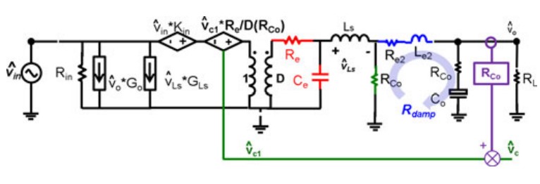
Fig. 2. Complete equivalent circuit model of constant on-time V2 control
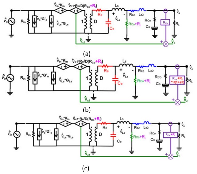
Fig. 3. (a) Enhanced constant on time V2 control (b) With high pass filter (c) With sensing capacitor current
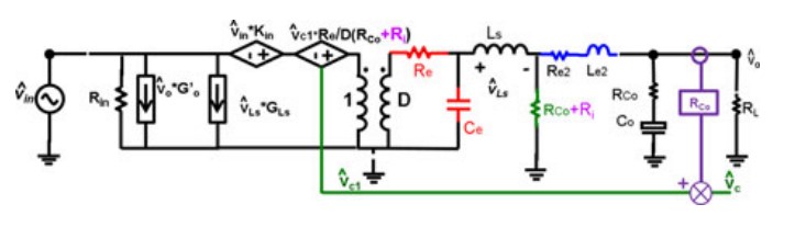
Fig. 4. Unified equivalent circuit model
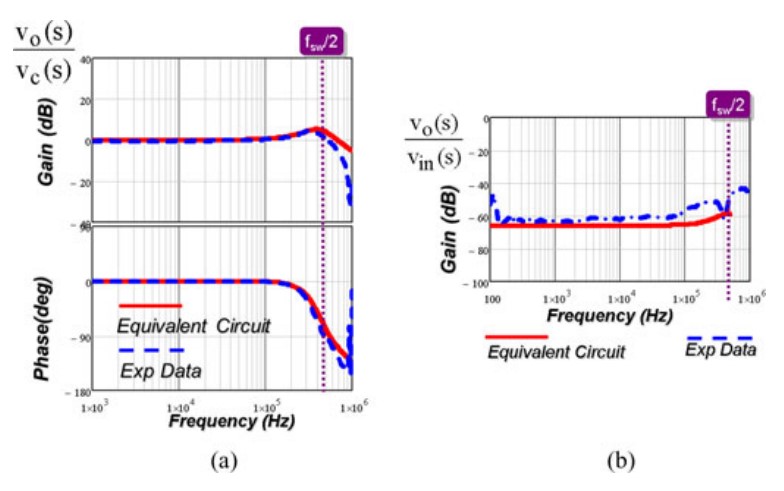
Fig. 5. Experimental verification of transfer functions
